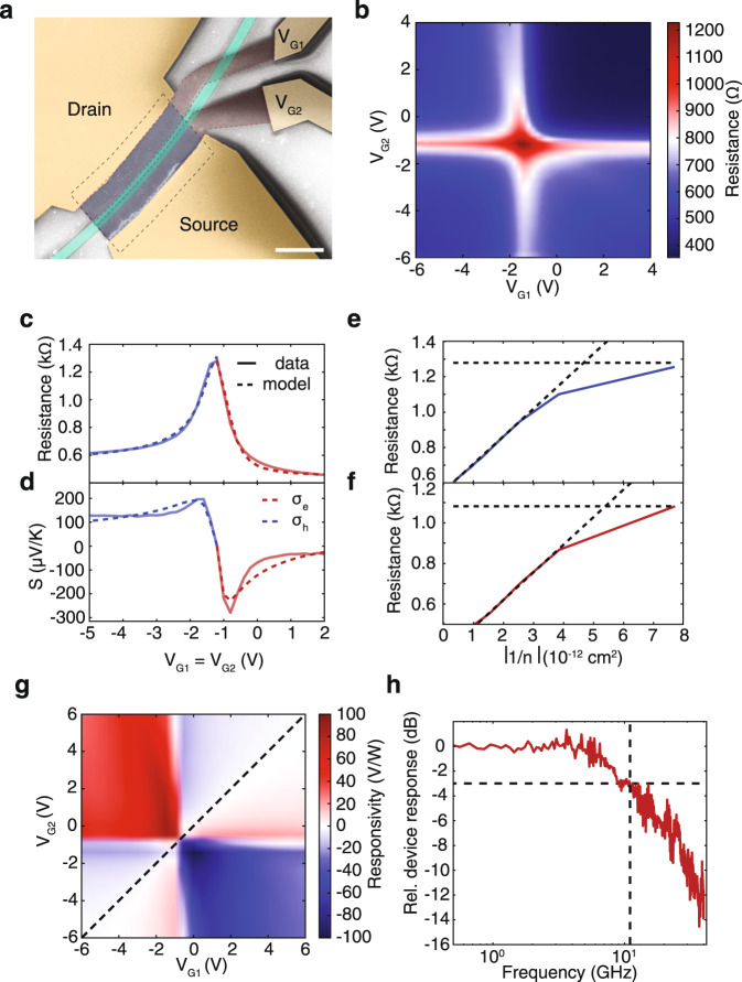
Fig. 4. GPD characterisation.
a False-colour SEM image of our GPD, showing Cr/Au contacts (yellow), Si WG (green), contacted hBN/SLG/hBN (blue, dashed line under contacts), and SLG gates (red). Scale bar: 2 μm. b Resistance map demonstrating independent tunability of charge carrier concentration in the SLG channel via VG1 and VG2. c Electrical characterization at homogeneous channel doping (solid lines, measured data; dashed lines, model). d Calculated S based on the electrical data in c. e, f) Resistance vs. inverse carrier concentration for e electron and f hole doping. g Photoresponse at zero bias on resonance (λ = 1555.87 nm). h Frequency response. The 3-dB cutoff frequency, marked by intersecting dashed lines, is ~12 GHz.

