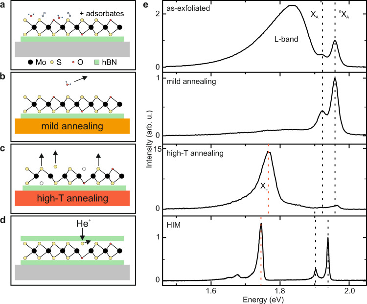
Fig. 1. Optical emission induced by adsorbates and engineered point defects in single-layer MoS2.
a Schematic of as-exfoliated single layer MoS2 on hBN (green) supported on a Si/SiO2 substrate (gray). Black (yellow) dots denote molybdenum (sulfur) atoms. Red dots denote oxygen atoms, which are present either as part of adsorbates or as substitutional atoms on sulfur sites. b Heating the substrate to mild annealing temperatures (Tannealing < 500 K, orange) removes the absorbates. c Heating the substrates to high annealing temperatures (Tannealing > 500 K, red) creates sulfur vacancies by thermal desorption (arrows). d Schematic of vacancy generation in MoS2 fully encapsulated in hBN through He-ion (He+) bombardment. e Evolution of low-temperature (T ∼20 K) photoluminescence spectra. As-exfoliated MoS2 exhibits a broad sub-gap luminescence (L-band) due to adsorbates. Mild annealing at Tannealing = 500 K removes these adsorbates suppressing the L-band. Upon annealing at Tannealing = 800 K, a narrow defect luminescence at 1.75 eV emerges (XL), due to the thermal generation of sulfur vacancies with well-defined in-gap states. Vertical, dashed lines indicate the emission energy of the neutral exciton (0XA), the trion (−XA), and XL. The intensities are normalized to the exciton transition 0XA. Helium-ion (He+) irradiation of MoS2 encapsulated in hBN using a helium ion microscope (HIM) generates a similar defect feature at 1.75 eV (T = 4.2 K).

