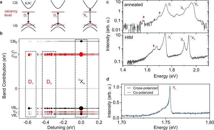
Fig. 4. Defect bound excitons in monolayer MoS2.
a Quasiparticle conduction (CB) and valence (VB) bands (black) near K-points and K′-points in the Brillouin zone of single-layer MoS2. The red lines denote states arising from sulfur vacancy levels. Arrows highlight the three types of excitonic transitions: between the delocalized bands (0XA), between the localized defect states only (D2) and between the valence band and the localized defect state (D1). b Band contribution to exciton transitions computed with GW-BSE. Dot size represents the relative oscillator strength, and the probability amplitudes of the occupied and empty bands contributing to it. Black indicates delocalized band states and red indicates localized defect states. CB0 and VB0, VB1 denote the dispersive unoccupied conduction and occupied valence bands (above and below the Fermi level), respectively. CD1 and CD2 are unoccupied localized defect levels, split by spin–orbit interaction arising from conduction band states. VD is the occupied localized defect level arising from the valence band. The three main peaks regions assigned with the D1, D2, and 0XA transitions are marked with dashed lines. c PL spectra of annealed and HIM-treated MoS2. The defect emissions occur in a range of 0.2–0.3 eV below XA with a dominant emission line (XL) around 1.75 eV. Further features (red arrows) are resolved at even larger detuning from the free exciton, in qualitative agreement with the predicted continuum of excitonic defect states below the pristine optical gap. d A single He-ion induced emitter shows no detectable valley polarization (T = 10 K, excitation energy 2.1 eV) as expected for transitions involving only defect levels (D2).

