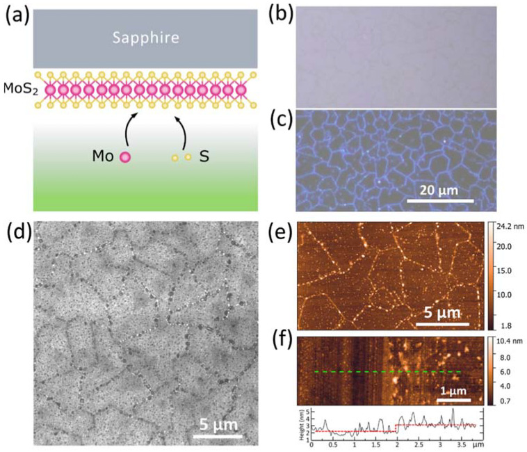
Figure 1.
(a) A schematic diagram showing the concept of MBE growth monolayer MoS2 on a sapphire substrate. (b,c) Optical image of the epitaxial MoS2 taken in bright field (b) and dark field (c) regimes. MoS2 covers more than 97% of the surface. (d) SEM image of the epitaxial MoS2 revealing the high crystallinity of the samples with the characteristic crystallite size 6 ± 2 μm. (e) The AFM topography map of MoS2 surface with a scan area of 17.5 × 10 μm2. Root mean square roughness of MoS2 is 0.5 nm in areas without defects. (f) The AFM topography map and the cross-sectional profile of the edge of epitaxial MoS2 along the green line, giving the MoS2 layer thickness of ~0.9 nm. The scan area was 5.5 × 2 μm2.

