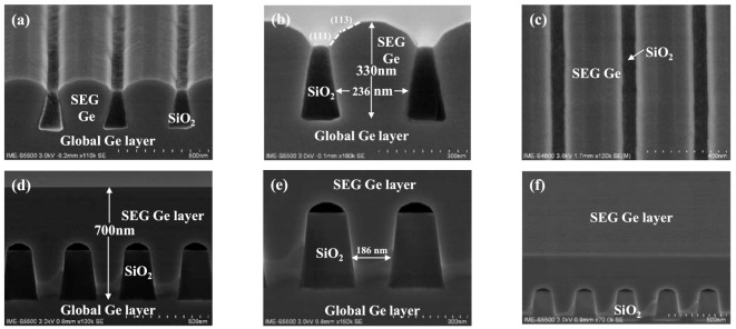
Figure 2.
(a–c) SEM cross-section images of selectively grown Ge layer on patterned Ge-on-Si substrate with the aspect ratio of 1.36: (a,b) 400 nm SEG Ge; (c) top view of sample in (a) or (b); and (d,e) 700 nm Ge layer grown on pattern with the aspect ratio of 1.67; (f) tilted planar view of sample (d).

