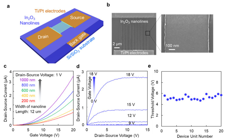
Figure 2.
The In2O3 nanolines FET device. (a) Schematic drawing showing the FET device. (b) FESEM images of the In2O3 nanoline area. (c) Transfer curve. The FET devices when varying the width of single line were measured. The drain-source voltage was 1 V. (d) Output curves. The back-gate voltages were increased from 0 V to 18 V. (e) Measured threshold voltages for 20 units of the In2O3 FET sensing device. The width of device is 800 nm.

