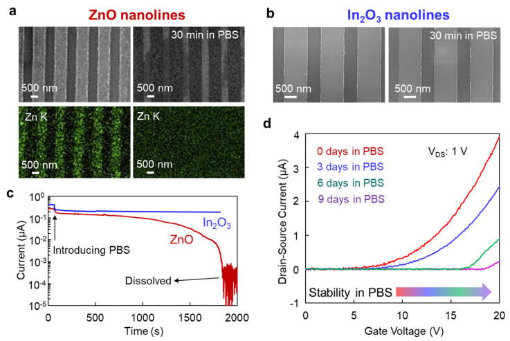
Figure 3.
(a) FESEM images and EDS elemental mapping images of ZnO lines before and after soaking in PBS solution for 30 min. (b) FESEM images of In2O3 nanolines before and after soaking in PBS solution for 30 min. (c) Time dependence of electrical conductance of In2O3 and ZnO nanolines when soaked in PBS solution. (d) Transfer curves of the In2O3 FET sensing device for different soaking times in PBS. Drain-source voltage was 1 V.

