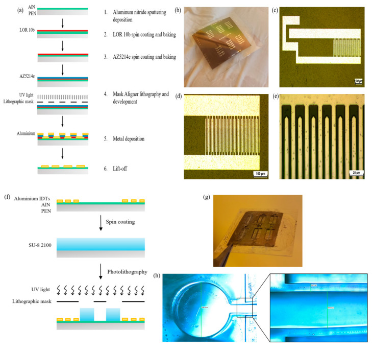
Figure 1.
Schematic representation of a bilayer photolithography process (a); fabricated SAW device (b) and relative electronic microscope images at 10× (c), 20× (d) and 100× (e); schematic representation of SU-8 microchannel photolithography (f), fabricated device (g) and its microscope images at 4× and 10× (h).

