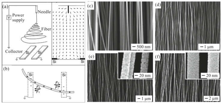
Figure 6.
(a) Schematic illustration of the setup for collecting nanofibers as a uniaxially aligned array. The collector contains an insulating void, such as the air gap between two strips of silicon wafers. (b) Electrostatic force analysis of a charged nanofiber spanning across two silicon strips. The orientation of the nanofiber is mainly controlled by the stretching force originating from the attractive electrostatic forces. (c–f) SEM images of uniaxially aligned nanofibers made of (c) carbon, (d) anatase TiO2, (e) NiFe2O4 and (f) TiO2/PVP. Reprinted with permission from [101]. Copyright 2003 American Chemical Society.

