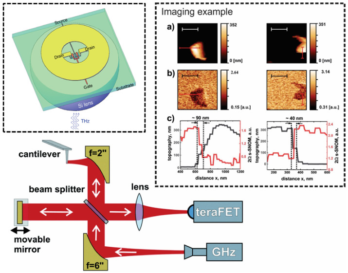
Figure 6.
Schematic of an all-electronic homodyne s-SNOM measurement setup with a detector based on a Si CMOS field-effect transistor. Left inset: 3D layout of the detector with the monolithically integrated annular ring antenna and the Si substrate lens. Active devices were fabricated using either a 90 nm or a 180 nm technology process node. The high sensitivity enables demodulation of the s-SNOM signal at up to the 10th harmonic of the cantilever’s oscillation frequency. Right inset: (a) AFM topography of a Si surface (black) with dielectric islands (brown); (b) simultaneously measured s-SNOM amplitude images recorded at the 2nd harmonic of the cantilever’s oscillation frequency. Scale bars in (a,b): 1 µm. (c) Line scans along the red lines in (b) showing a spatial resolution down to <50 nm. Figure modified from Ref. [318].

