Figure 2.

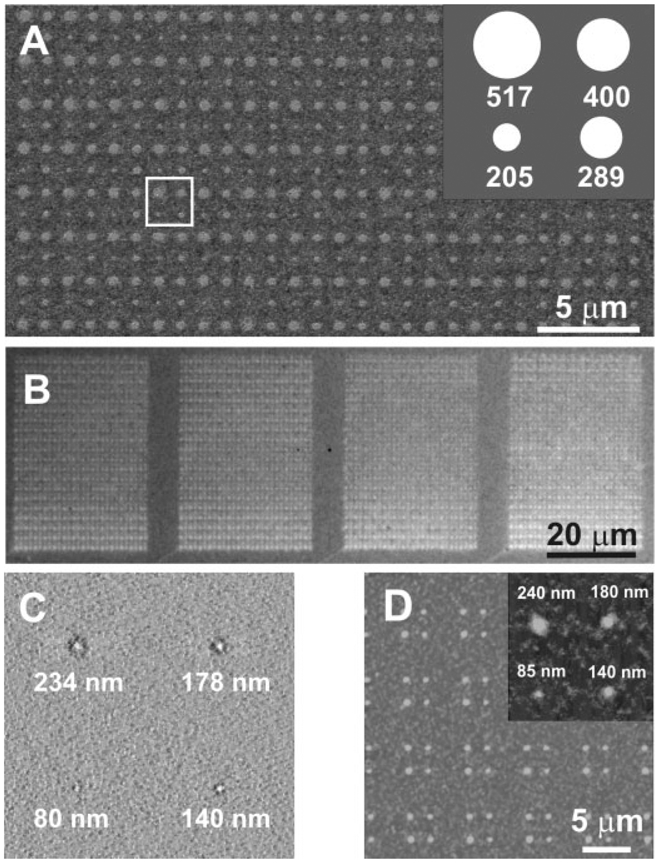
A) SEM and B) optical microscopy images of the generated positive Au nanostructures; C) contact-mode AFM image of PEG patterns used as etch resist to make the dot features in (D); D) tapping-mode AFM images of positive dot solid-state Au nanostructures generated from (C). One cell, which is designated by the white box in (A), is shown schematically in the inset of (A). The inset in (D) shows a zoomed-in AFM image of a generated Au dot array.
