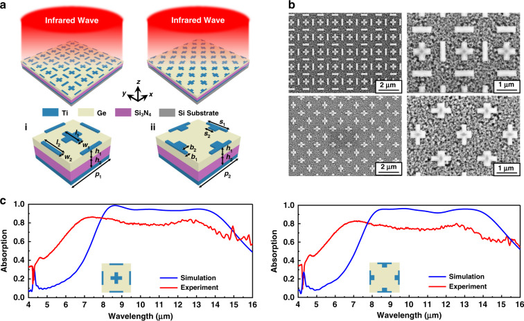
Fig. 3. Absorption characteristics of two types of Ti/Ge/Si3N4/Ti absorbers.
a Schematic of two types of Ti/Ge/Si3N4/Ti absorbers (h1 = 270 nm, h2 = 330 nm, p1 = 1.6 μm and p2 = 1.8 μm): (i) the top layer consists of periodic nano-cross and nano-strip structures (l1 = 630 nm, w1 = 200 nm, l2 = 750 nm and w2 = 100 nm); (ii) the top layer consists of irregular nano-cross structures (s1 = 850 nm, b1 = 100 nm, s2 = 300 nm and b2 = 200 nm). The thickness of the top Ti layer is 22 nm, and the bottom Ti layer is 120 nm, where is thicker than its penetration depth. b SEM images of two types of fabricated Ti/Ge/Si3N4/Ti absorbers. c Simulated and experiment absorption spectra of the two types of Ti/Ge/Si3N4/Ti absorbers

