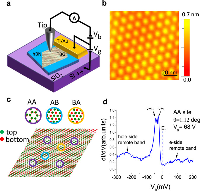
Fig. 1. STM/ STS on magic-angle twisted bilayer graphene.
a Schematic of the STM device and measurement setup. The TBG sample was made using the “twist and stack” method. The Tungsten tip is kept grounded while a bias voltage is applied to the sample. A backgate voltage is applied between the p-doped silicon backgate and the sample. All measurements were taken at 4.9 K. b STM topography measured at a bias of −300 mV and tunneling current of −30 pA. The bright yellow spots which form a triangular lattice are the AA stacking regions. The surrounding darker orange regions have approximately AB and BA stacking. The moiré wavelength was measured from STM topography to be 12.6 nm which corresponds to a twist angle of 1.12°. c An illustration of the various stacking arrangements. The green and red dots represent the carbon atoms in the top and bottom Graphene layer respectively. d shows a typical spectrum measured at the center of an AA region at = 68 V when the flat bands are completely full. The van Hove singularities (VHS) and the remote bands on either side of the flat band are labeled. Gap-like dips in the signal separate the flat bands from the remote bands. The Fermi level of sample is shown with a dashed line at .

