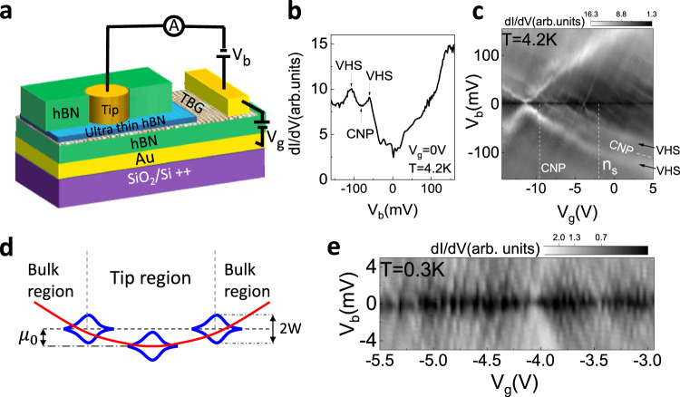
Fig. 4. Carrier confinement in a TBG planar tunneling device.
a Schematic of the planar tunneling device. An ultra-thin hBN acts as a tunneling barrier between the metallic tip and the TBG. b Tunneling spectrum measured at 0 V backgate voltage showing the flat bands. The sample is highly n-doped because of the work function difference between the tunneling electrode and the TBG. c Gate dependence map of the STS. Flat bands can be seen as two bright parallel lines at negative bias. The other features are a result of confinement. d Schematic of the position dependence of the charge neutrality point. is the shift in the charge neutrality point under the tip compared to the bulk region. e High resolution gate dependence maps measured at 0.3 K showing coulomb diamonds, a result of electron confinement.

