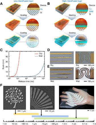
Fig. 1. Dry transfer printing by interfacial thermal stress control and antiatomic diffusible interface design.

(A) Schematic illustration of the process for dry transfer printing depending on the atomic diffusion level of the material with a high CTE. The process is classified into a low-interdiffusion layer (Au) and (B) a high-interdiffusion layer (Cu), necessitating an antiatomic diffusion layer. (C) Computational and theoretically calculated results for the scale-release time correlation of wet and dry transfer printing denoted by the blue line and red line, respectively. Dry transfer printing takes only a few hundred milliseconds to release submeter-scale patterns. (D) Optical images of line and serpentine patterns in the dry transfer printing process and (E) pattern floating and distortion in the wet transfer printing process. Photo credit: Seungkyoung Heo, Daegu Gyeongbuk Institute of Science and Technology. (F) Optical images of patterns with diverse shapes (tree pattern, radial pattern, and fern leaf fractal pattern) from the nanometer scale to the submeter scale by dry transfer printing. Photo credit: Seungkyoung Heo, Daegu Gyeongbuk Institute of Science and Technology.
