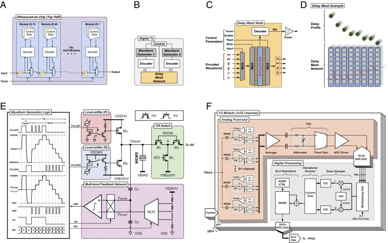
Fig. 2.
UoC schematics. (A) Module-level communication architecture. (B) Digital transmit waveform and delay controller. (C) Delay mesh node at each MEMS element. (D) Delay mesh network example delay profile. (E) Schematic of the multilevel pulser with tunable slew rate and its timing diagram. (F) Modular on-chip receiver design with analog circuitry supporting each group of eight elements in the analog front end. The transmit pulser and receive TIA circuitry are unique for each element. Element signals can be combined and share DC offset correction, dynamic TGC with arbitrary profile and analog-to-digital conversion (ADC) operations. Digital processing downstream of the ADCs performs baseband conversion for data reduction while preserving important signal content. Signals can be combined or separated in a variety of ways before being written to memory for offload.

