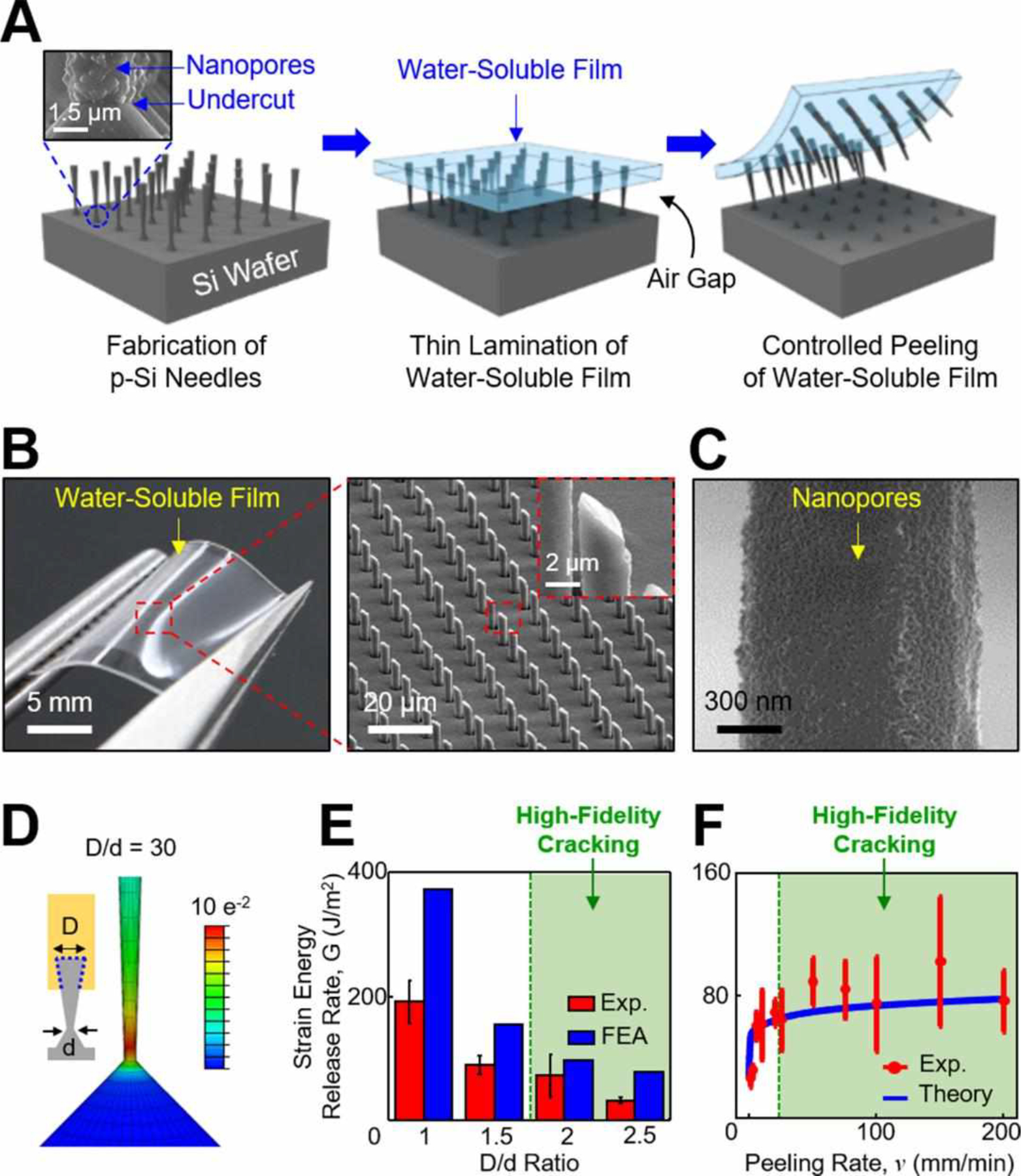
Figure 1. Design principle and fabrication process.

(A) Schematic illustrations for the construction of the p-Si needles on a water-soluble backing. The inset image highlights the bottom undercut and nanopores at the bottom and on the surface of the p-Si needles, respectively. (B) Optical images of the p-Si needles integrated with a PVA film. The inset image highlights the sharpened angular tip of the p-Si needles. (C) SEM image of the nanopores formed on the surface of the p-Si needles. (D) Representative FEA results showing the distribution of principal strains along the p-Si needle during constant peeling. (E) Experimental and FEA results for the effect of D/d ratio on strain energy release rate (G). (F) Experimental and theoretical results for the effect of peeling rate (v) on G.
