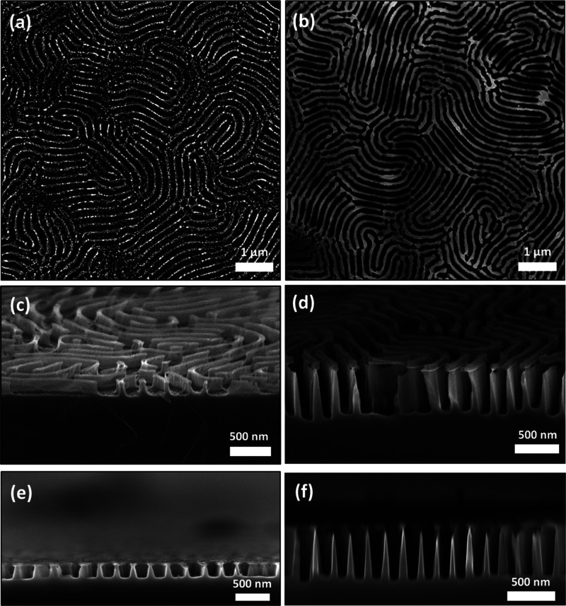
Figure 7.
SEM images of Si nanowall after pattern transfer. Top-down SEM images of Si nanowall structures following an ICP etch of the iron oxide hard mask for (a) 1 and (b) 3 min etch, with tilted images (70°) shown in (c,d), respectively. (e,f) Cross-sectional SEM image of Si nanowalls for samples (a,b).

