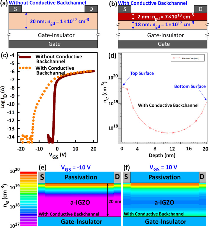
Figure 6.
TCAD simulation of the effect of deep UV light radiation on a-IGZO TFTs. (a and b) Schematics representing the TFT models used to simulate TFT characteristics (a) before and (b) after deep UV light radiation. A 2 nm thick a-IGZO film with a donor concentration (ngd) of 7 × 1018 cm-3 is used to simulate the photoionization of neutral oxygen vacancies at the top surface of the a-IGZO film. ngd for the bulk is 1 × 1017 cm-3. (c) Simulated transfer characteristics. (d) Line profile of the electron concentration (ne) from the top to the bottom surface when VGS = 10 V. (e and f) Images showing the distribution of ne in the a-IGZO with a conductive backchannel when (e) VGS = − 10 V and (f) VGS = 10 V. The presence of a conductive top surface induces a negative ΔVTH and the “hump”.

