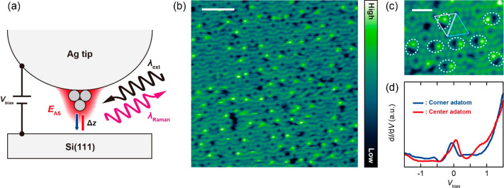
Figure 1.
(a) Schematic of the experiment. EAS illustrates the extreme plasmonic field occurring at the atomic-scale protrusion at the tip apex. (b) STM image of Si(111)-7 × 7 under illumination (10 K, Vbias = 0.3 V, ISTM = 1 nA, λext = 633 nm, Pext = 0.7 W/cm2, scale bar = 5 nm). (c) Enlarged STM image (scale bar = 1 nm). The bright/dark pairs are indicated by the dashed ellipses. The faulted/unfaulted half unit cell is indicated by the pink/blue triangle. (d) Conductance spectrum measured under illumination (10 K, set-point: Vbias = 0.5 V, ISTM = 0.1 nA, λext = 532 nm, Pext = 0.15 mW/μm2).

