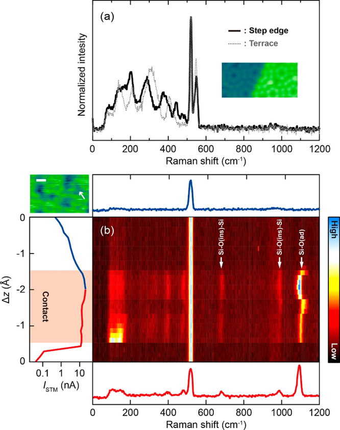
Figure 3.

(a) APC-TERS at the step edge of the Si(111)-7 × 7 surface (10 K, Vbias = 0 V, λext = 633 nm, Pext = 0.7 mW/um2). The gray dashed line is the averaged spectrum over the terrace. The inset shows the STM image of the step edge. (b) APC-TERS at oxidized region of the Si(111)-7 × 7 surface (10 K, Vbias = 0 V, λext = 532 nm, Pext = 1 mW/μm2). The left panel shows the simultaneously recorded ISTM–Δz curve. The red shaded region indicates the APC. The top and bottom panels display the TERS spectra in the tunneling and contact regimes, respectively. The STM image of the partially oxidized surface is shown in top-left (scale bar is 2 nm). The position for APC-TERS measurement is indicated by the arrow.
