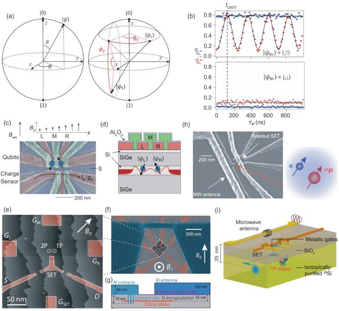
Figure 1.
Single- and two-qubit gate control and devices for semiconductor qubits. (a) Bloch-sphere representation of a qubit. A superposition state  can be represented by a point on the sphere (left). An arbitrary rotation from the initial state
  to the target state
  can be decomposed by successive rotations about the z and y axes for φz and φy, respectively (right). (b) The spin-up probability of the spin-up state for the right qubit
  (blue) and the left qubit
  (red) as a function of interaction time
  for input states
  and
and  . The vertical dashed line at
  corresponds to a CNOT gate. (Adapted from [17].) (c) and (d) are a false-color SEM image and a schematic cross-section of a Si/SiGe DQD, respectively. The DQD with two electrons confined in the potential created by gates L, M and R is used to form two spin-1/2 qubits and a SET under the DQD is used to work as a charge sensor. A slanting Zeeman field was created by a micro-magnet (not shown) for qubit control. (Adapted from [17].) (e), (f) and (g) are images and schematics for the device fabricated by STM hydrogen lithography. (Adapted from [30].) (e) Large-scale STM image of the device; red areas are P-doped to form a SET, source and drain leads, and electrostatic gates. A donor molecule (2P) and single donor (1P) are shown by two circles. (f) False-color composite SEM and STM image showing the buried donor structures (red) and the aluminum antenna (blue). (g) Vertical cross-section of the donor device, showing the thicknesses (not to scale) and relative positions of the silicon, phosphorus, oxide and aluminum layers. (h) and (i) are a SEM image and schematic oblique view of a device fabricated by ion implantation, highlighting the position of the P donor, the MW antenna and the readout SET. (Adapted from [31] and [51].)

