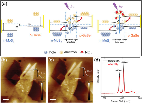
Figure 4.

a) Schematic diagram of the sensing mechanism of the heterojunction. Band diagram of isolated MoS2 and GaSe (left), heterojunction between the two materials under light illumination (middle) and the heterojunction with NO2 exposure (right). KPFM images of the heterojunction b) before and c) after exposing to NO2. Scale bars are 5 µm. d) Raman spectra of the heterojunction before and after NO2 exposure at room temperature.
