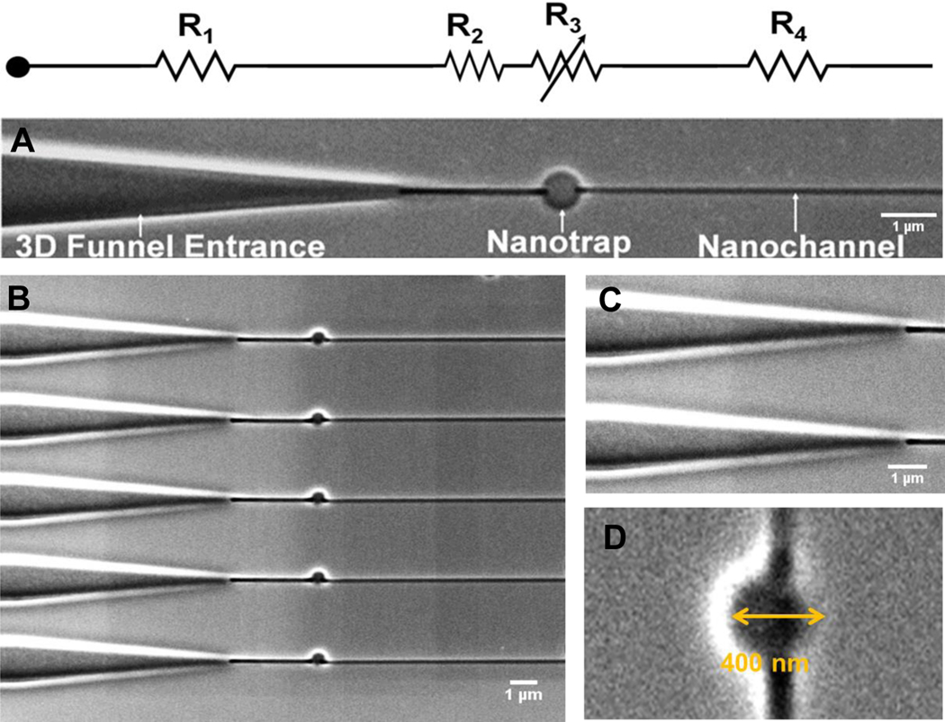
Figure 2.
(A) SEM images of the multi-structured nanofluidic circuit comprised of a 3D funnel, nano-trap, and a stretching nanochannel. Its equivalent circuit diagram with resistors including an adjustable resistor for the nano-trap (variable resistance is predicated on changing the trap size) is also shown. (B) Array of multi-structured nanofluidic circuits for high throughput processing of single DNA molecules to search for AP sites. (C) Entrance funnel used to extend the electric field into the adjoining microchannel for assisting in loading single DNA molecules into the nanofluidic circuit from access microchannels. (D) SEM image of a 400 nm nano-trap (diameter and depth). The device shown was made from PMMA using thermal NIL from a resin stamp produced via UV-NIL from a Si master.

