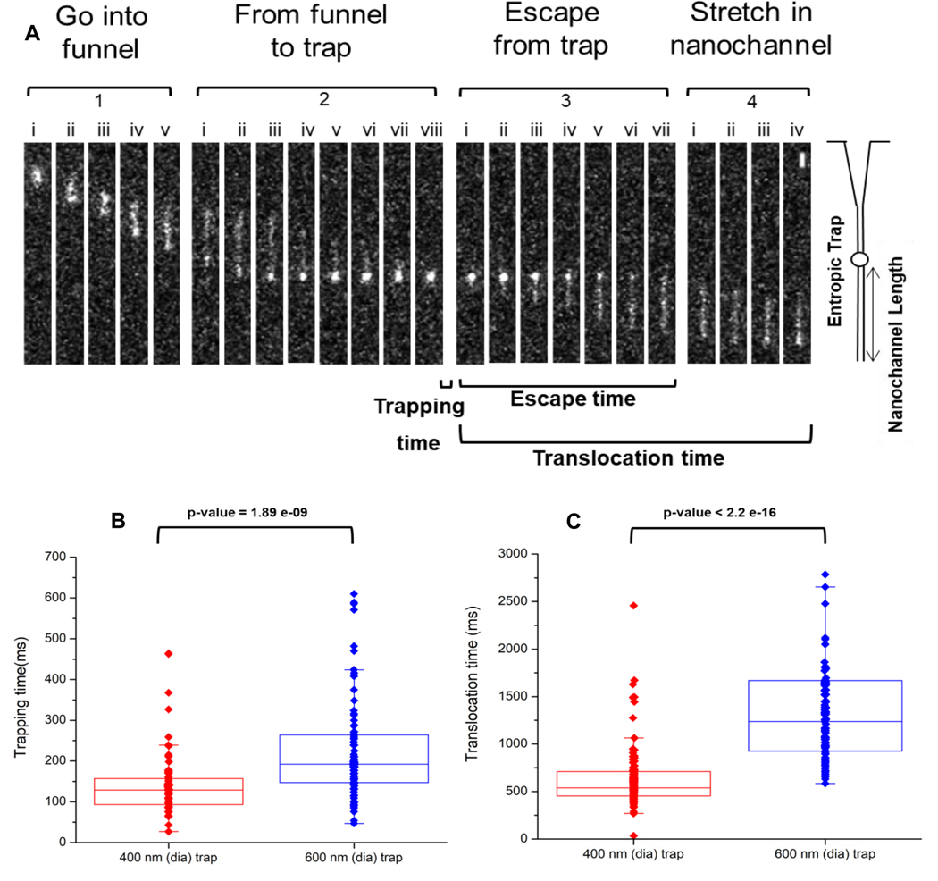
Figure 3.
(A) Representative frames showing the translocation of stained λ-DNA through the multi-structured nanofluidic circuit. The frames were divided into 4 sections; (i) ‘Enter the funnel,’ where the DNA enters the funnel from the microfluidic channel and into the nanofluidic circuit. (ii) ‘From the funnel to trap,’ where the DNA leaves the funnel, stretches briefly in the short nanochannel section and enters into the nano-trap. (iii) ‘Escape from trap,’ where the DNA resides in the trap for a period of time and subsequently ejected from the nano-trap and inserted into the stretching nanochannel. (iv) “Stretching of dsDNA” in the stretching nanochannel to near its full contour length and is parked so as to detect the AP sites. For these experiments, the driving voltage was 0.1 V DC and the buffer used was 1× TBE (pH = 8.0). The scale bar (5 μm) is shown in Section 4, image (viii) at the top right corner of the image. Box plots showing (B) trapping and (C) translocation times of λ-DNA electrokinetically transported through the multi-structured nanofluidic circuit under a 0.1 V driving voltage having a 400 nm or 600 nm trap. The average trapping time for the 400 nm trap was ~138 ms, while for the 600 nm trap it was 225 ms. The average translocation time through the nanofluidic circuit with a 400 nm trap was 660 ms, while for the 600 nm trap it was 1847 ms. All measurements were performed using 1X TBE buffer (pH = 7.9). Events were captured at 10 ms exposure times resulting in a frame rate of 90 fps and 1 × 1 binning for the EMCCD. The p value calculated between the 400 and 600 nm traps for the trapping and translocation times (Wilcoxon signed rank test) were statistically different at the 95% confidence interval (p<0.05).

