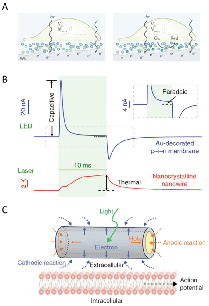
Figure 4.

Mechanisms of photoresponses for semiconductor-based nano-bioelectronic devices. A) Illustrations of the photocapacitive (left) and photofaradaic (right) response from the semiconductor working electrode, labeled WE, in biological settings. Electrode-electrolyte interfaces form electrical double layers. The capacitive response occurs when photostimulation induces a capacitive discharge of the double layer, producing a relatively large, transient current. The photofaradaic response comes from the steady rate of charge transfer due to redox reactions taking place with accumulated charge carriers from illumination. Adapted with permission.[82] Copyright 2018, Springer Nature. B) Traces of photocapactive, photofaradaic, and photothermal responses in planar diode junctions and silicon nanowires, respectively. The photothermal response is a consequence of nonradiative recombination in the depletion zone. Adapted with permission.[60] Copyright 2018, Springer Nature. C) Schematic of the photofaradaic response with coaxial p-i-n SiNWs. Electrons on the n-type shall facilitate reduction reactions around the NW surface, while holes that accumulate in the p-type zone can only participate in oxidation reactions on the exposed shell regions on the NW ends. Adapted with permission.[44] Copyright 2018, Springer Nature.
