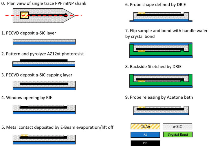
Figure 1.
Sketch of a single trace PPF mINP shank for process illustration purposes. (0) Top view of completed device; dashed line shows cross-section cut for (1–9). (1) Starting with an oxide-coated Si wafer, an a-SiC film is deposited via PECVD. (2) Positive photoresist is spun, patterned and thermally annealed to pyrolyze the photoresist into PPF carbon traces. (3) Wafer is coated with another layer of a-SiC. (4) RIE is used to open windows exposing the recording tip and bonding pad. (5) Metal is deposited on the bond-pads using a lift-off process and (6) probe is defined by DRIE (mINP only, singled ended electrode process completed at step (5)). (7) Die is flipped and bonded to Si handle wafer using crystal bond. (8) Backside Si is thinned to ~50 µm by DRIE. (9) Probes are released from Si handle wafer via crystal bond dissolution in Acetone.

