

Abstract
Synthetic antiferromagnets (SAFs), composed of Ru spacer with a Re insertion layer, reveal superior thermal stability up to 450 °C annealing, making the back-end of line process a wider manufacturing window and tolerance to integrate the perpendicular magnetic tunneling junctions (P-MTJs) into CMOS process. The coupling strength decays significantly for SAFs with single Ru spacer after annealing above 400 °C. Due to the characteristics of refractory metals, Re can behave as a diffusion barrier during annealing. Furthermore, the Re spacer can still keep reasonable RKKY coupling strength. Therefore, the SAFs with Ru/Re composite spacers exhibit higher RKKY coupling strength than Ru spacers after 450 °C annealing. In addition, we discovered the different enhancements for the upper and lower interfacial Re insertion, which was attributed to the varied defect formation at interfaces. The stacking fault was formed at the upper Ru/Co interface in as-deposited state. When Re was inserted at the upper interface, the diffusion between Co and Ru was significantly suppressed and the stacking fault can be eliminated during annealing, leading to enhanced interlayer coupling. Through the interfacial engineering, we may have more degrees of freedom to tune the SAF performance and thus enhance process compatibility of P-MTJ to the CMOS process.
Subject terms: Magnetic properties and materials; Surfaces, interfaces and thin films
Introduction
Synthetic antiferromagnets (SAF) have played an indispensable role in magnetic tunnel junctions (MTJs) for the applications of magnetic random access memory (MRAM). For high density MRAM, MTJs are typically composed of CoFeB layers with perpendicular magnetic anisotropy1. To eliminate the stray field on the free layer, which is generated from the reference layer and may lead to asymmetric switching current density, synthetic antiferromagnetic layer (SAF) with nearly zero magnetization is used as the reference layer2,3. SAF is composed of two magnetic layers separated by a spacer with compensation of net magnetic moment through the Ruderman–Kittel–Kasuya–Yosida (RKKY) interaction4–7. In addition, the interlayer coupling may enhance stability of the reference layer and prevent it from writing error.
Nowadays, Ru is the most widely utilized material for RKKY spacer in MTJs with large interlayer coupling strength and a suitable crystal structure for perpendicular [Co/Pt]n multilayers as the reference layer8. Typically, the Ru thickness is in the range of 0.35–0.45 nm and 0.8–1.0 nm, locating at the 1st and 2nd peaks of RKKY oscillation, respectively, with the coupling strength around 2.0 and 1.0 erg/cm29,10. The strongest coupling can be achieved by using the Ru thickness at the 1st peak, however, the thickness control is in a stringent window for fabrication. In addition, to integrate MTJ into CMOS process, an annealing step upon 400 °C or even higher temperature in the back end of line (BEOL) process is required, which may degrade the magnetic properties of MTJ. Since the RKKY coupling, the most important indicator for SAF performance, strongly depends on the interface conditions, this high-temperature annealing may cause significant reduction of the interlayer coupling strength Jex due to the inter-diffusion at the interface between ferromagnetic and Ru layers10–12. Recently, Ir has been reported as an alternative spacer, which reveals stronger coupling strength and better thermal durability than Ru. The Ir spacer with the thickness 0.48 nm shows Jex of 1.9 erg/cm2 after 400 °C annealing13. However, the price of Ir is much higher than that of Ru in material markets. Therefore, searching for the practical and affordable solution of spacer is a key challenge for MRAM mass production.
To prevent diffusion during the high temperature annealing, building a diffusion barrier is an intuitive and effective method. One potential approach is to engineer the interface between Ru and ferromagnetic layers by inserting a thin diffusion barrier. To select a thermally stable material, melting point is a good indicator. Although Mo, Ta and W are of high melting point materials, as known as “refractory metals”, their negligible RKKY coupling and body-centered cubic (BCC) structure are not suitable for the conventional reference layer [Co/Pt] /Ru with face-centered cubic (FCC) and hexagonal close-packed (HCP) structures. On the other hand, another member of refractory metals, Re has a quite high melting point with a HCP structure. Furthermore, Re possesses the forth strongest RKKY coupling strength, while the top three are Ru, Ir, and Rh14. Although the coupling strength of Re is not as strong as the top three, it is not negligible like other refractory metals. In this work, we demonstrate a composite spacer composed of Ru and Re, in which Re can reach high thermal durability and still remain RKKY anti-ferromagnetic coupling after annealing upon 450 °C. By optimizing the layer structure, the composite spacer exhibits even higher coupling strength than Ru spacer after 450 °C annealing. Furthermore, since Ru is an essential material for various applications, its large demand in material market leads to a much higher price than Re. Therefore, by engineering Ru interface, we may not only enhance thermal durability of SAFs but manufacture the MTJs in a price-friendly way.
In addition, we also discovered the different enhancements for the upper and lower interfacial Re insertion, which was attributed to the varied defect formation at interfaces during annealing. By the microstructural analyses, we demonstrate that the insertion of Re at the upper interface can eliminate the stacking faults during the annealing, leading to enhanced interlayer coupling. Our findings provide a clear guideline to tune the SAF performance through the interfacial engineering, and can further enhance process compatibility of perpendicular MTJ to the CMOS process.
Results and discussions
Structure design
We prepared SAF samples with the structure shown in Fig. 1. Based on the typical SAF structure [Co/Pt]n/Ru/[Co/Pt]n with perpendicular anisotropy, we additionally insert thin Re film at the interfaces between Ru and Co. As a diffusion barrier, the Re film is expected to perform high thermal durability to prevent interlayer diffusion. The samples were then annealed with varied temperatures up to 450 °C for 1 h, compatible with the thermal budget of BEOL used in CMOS process.
Figure 1.
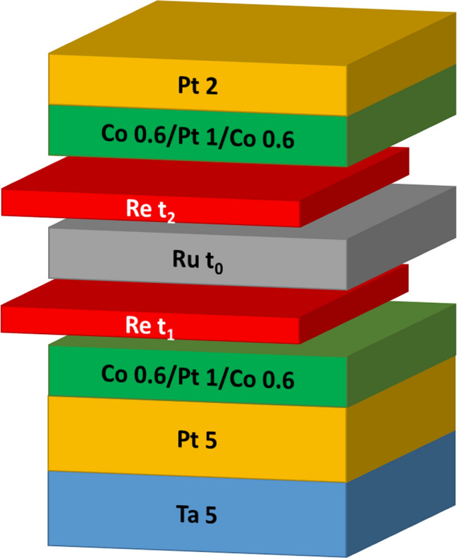
Schematic diagram for film stack of the SAF layer. Re is inserted at top and/or bottom of Ru. The numbers represent layer thickness in nanometers.
Magnetic properties of SAFs
We first prepared the samples with a sandwich structure, Re/Ru/Re, in which two Re layers were fixed at 0.18 nm and Ru was varied. The Re layer is about one monolayer inserted between Ru and Co. The sample with a single Ru spacer is also made for comparison. The hysteresis loops were measured by using VSM and the interlayer coupling strength Jex was determined by the following formula9,15,16
Ms is saturation magnetization of the ferromagnetic layer and t is thickness of ferromagnetic layers. Hex, the exchange field strength induced by antiferromagnetic coupling, is the loop shift along the x-axis (field-axis) of M-H loop. The Jex value is plotted as a function of total spacer thickness in Fig. S1 of Supplementary Information. Compared to the sample with a single Ru spacer, the sample with composite spacer reveals similar dependence of interlayer coupling on the spacer thickness, which has a maximum Jex value around 0.79 nm (Ru 2nd RKKY anti-parallel coupling peak). This result indicates that the fixed spacer thickness at 0.79 nm for the composite spacer may still provide the highest coupling strength. Since RKKY strength strongly depends on the spacer thickness, we believe that it is proper to fix the composite spacer at the same thickness for fair comparison with a single Ru spacer. Therefore, for our experimental design, we made all the samples composed of various composite spacers with the same total thickness (0.79 nm). On the other hand, the Jex generated by the Re/Ru/Re spacer was smaller than that by a single Ru spacer because Re provides less coupling strength. Therefore, the bilayer structure with only one side Re is a possible way to reach a balance between the Jex value and thermal durability.
The sample with a composite spacer, Ru 0.61 nm/Re 0.18 nm, was made to compare with one consisting of a single Ru (0.79 nm) spacer and their hysteresis loops before and after 450 °C annealing are shown in Fig. 2. In the as-deposited state, the largest Hex 6.5 kOe for the sample with a single Ru spacer can be achieved, shown in Fig. 2a, which corresponds to the Jex of 1.02 erg/cm2, comparable to the reported value at 2nd RKKY peak10. The interlayer coupling Jex is slightly decreased to 0.93 erg/cm2 for the as-deposited sample with the Ru/Re composite spacer, shown in Fig. 2a. After annealing at 450 °C for 1 h, Jex degrades to 0.35 erg/cm2 for the sample with a single Ru spacer (Fig. 2b), but the Jex value of the sample with a composite spacer is only reduced to 0.57 erg/cm2. With the less reduction on Jex, the composite spacer shows more robust thermal durability and keeps relatively good Jex after 450 °C annealing.
Figure 2.

M-H loops of [Co/Pt]n based SAFs. Black curve is for the sample with a single Ru spacer of 0.79 nm and red one is for the sample with a composite spacer of Ru 0.61 nm/Re 0.18 nm. (a) As-deposited state (b) After 450 °C 1 h annealing.
Effects of Re insertion on RKKY coupling strength Jex
To further explore effects of Re insertion, we prepared the SAF samples with various composite spacers. We made two types of insertion, Ru/Re and Re/Ru, that is, insertion of Re in the upper or lower interface, respectively. In addition, we varied the Ru thickness from 0.18 to 0.61 nm but kept the total spacer thickness about the same (0.79 nm), locating at the region of 2nd AF coupling peak of single Ru. Figure 3a displays the dependence of Jex on Re thickness for the as-deposited and annealed samples. In both spacers, Jex has highest value at Re 0.18 nm (Ru 0.61 nm) and remains similar strength at Re 0.29 nm (Ru 0.50 nm). Jex decreases with further increasing Re thickness, which may result from the smaller RKKY coupling strength of Re. On the other hand, the upper Re insertion (Ru/Re spacer) exhibits higher Jex than the lower Re insertion (Re/Ru spacer). Since Jex strength strongly depends on the Ru (0002) texture grown on (111)-oriented [Co/Pt]n multilayers17, we speculate that the thin Re insertion on the top of [Co/Pt]n (the lower insertion case, Re/Ru) may slightly deteriorate the subsequently deposited Ru crystallinity, resulting in a lower Jex. After 450 °C annealing, Jex of all samples drops obviously. To verify the crystallinity of Ru and Re, we prepared samples of Si/SiO2//Ta 5/Pt 2/Co 0.6/Re (or Ru) 5 nm for XRD measurements, as shown in Fig. S2 of Supplementary Information. The sample with Re shows quite weak signal unlike strong textured Ru, which is consistent with the previous report that Re was not easy to be crystallized when the film thickness is too thin18. Therefore, we suggest that very thin Re in our layer structure may grow in relatively poor crystallization on the [Co/Pt]n, which slightly deteriorates the following Ru texture. On the other hand, if Ru grows first, the (0002) texture is well established so the following Re can also have (0002) textured growth due to the proper Ru seed layer. Therefore, the different interfacial conditions may lead to various Ru crystallinity, which gives rise to different Jex for composite spacers of Ru/Re and Re/Ru.
Figure 3.

Effects of Re insertion on RKKY interlayer coupling. (a) Variations of Jex with Re thickness. The total thickness of the spacer is fixed at 0.79 nm. Red and blue lines represent the Re upper (Ru/Re) and lower (Re/Ru) insertion, respectively. Solid and open circles represent for as-deposited and annealed states, respectively. (b) Jann/Jas-dep presents Jex changes after annealing of Ru/Re (red) and Re/Ru(blue) spacer.
To look into details of the changes after annealing, we plot the ratio of Jex changed after annealing, Jex (annealed)/Jex (as-deposited), shown in Fig. 3b, which may indicate the degree of degradation due to inter-diffusion. A higher ratio was observed for thicker Re, suggesting the diffusion is less for thicker Re spacer. In addition, the sample with the upper insertion of Re (Ru/Re spacer) shows better performance, implying that the inter-diffusion may be more severe at the upper interface of spacer so that the suppression of inter-diffusion by upper Re works more effectively.
We then compare the annealing temperature dependence of Jex for different spacers, as shown in Fig. 4. Compared to the single Ru spacer, the upper insertion (Ru/Re spacer) shows better thermal durability. Although the as-deposited sample with the Ru/Re spacer possesses a slightly lower Jex, Jex of the sample with Ru/Re spacer drops slowly and remains a higher value than that of the sample with a single Ru spacer after annealing. In contrast, the thermal durability of lower insertion (Re/Ru spacer) is not as good as Ru/Re. The degradation rate of Jex for the sample with the Re/Ru spacer is similar to that with the Ru spacer up to 400 °C annealing. In addition, the Jex of Re/Ru in the as-deposited state is much lower so that the Jex value of annealed samples is less than that with the Ru spacer for the annealing temperature lower than 450 °C. As we discussed earlier, the insertion of thin Re at the lower interface might deteriorate the Ru crystallinity, leading to the reduced Jex.
Figure 4.
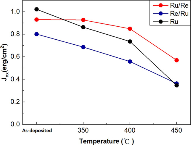
Variations of Jex with different annealing temperature. Red and blue lines are the Jex for the sample with the Ru/Re and Re/Ru spacers, respectively. The thickness for Ru and Re is 0.61 and 0.18 nm, respectively. Black line is the Jex for the sample with Ru spacer (0.79 nm).
We also prepared the sandwich spacer composed of Re 0.18 nm/Ru 0.43 nm/Re 0.18 nm. The Jex value is 0.65 erg/cm2 in the as-deposited state and becomes 0.40 erg/cm2 after 450 °C annealing, slightly higher than the Ru spacer (0.35 erg/cm2) but lower than that of the Ru/Re spacer (0.57 erg/cm2). Although the insertion of both Re layers may further suppress the inter-diffusion, the deteriorated Ru crystallinity due to the lower insertion and reduced Ru thickness may compensate the gained thermal durability. Consequently, the SAF with the Ru/Re spacer, which can have strong RKKY interaction provided by Ru directly contacting to the ferromagnetic layer at the lower interface and build a barrier to slow down the inter-diffusion at the upper interface, can achieve the highest Jex after high temperature annealing.
Effects of annealing on interfacial roughness and microstructure
In order to quantize the interfacial difference and the function of Re during annealing, we use X-ray reflectometry (XRR) analysis. Because of complicated multilayer structure, it is not easy to fully fit the experimental data of XRR. Therefore, we prepared samples in simplified structures to highlight the interface we would like to investigate. Three samples were grown: sub//Ta 5/Pt 5/Ru 5/Co 0.6/Pt 5 (sample A), Ta 5/Pt 5/Ru 5/Re 0.18/Co 0.6/Pt 5 (sample B), Ta 5/Pt 5/Co 0.6/Ru 5 (sample C) and Ta 5/Pt 5/Co 0.6/Re 0.18/Ru 5 (sample D). The interface we are interested in is underlined. Sample A (C) corresponds to the case for top (bottom) interface of a single Ru spacer in SAF structure. Sample B (D) corresponds to the case for upper (lower) Re insertion of a composite Ru/Re (Re/Ru) spacer in SAF structure. XRR results for the as-deposited samples and samples annealed at 450 °C, shown in Fig. 5, reveal clearly oscillating spectra. By fitting the spectra, we can get the information of interfacial roughness19. Since the sample structure is quite similar, after the spectra fitting, we mainly focus on the interfaces at Ru (Re) contacting the ferromagnetic layer. In sample A case, the fitted roughness at Ru/Co (top interface of Ru) is 0.39 nm for as-deposited state and 0.55 nm for annealed state, respectively, shown in Fig. 5a,b. The 0.16 nm increased roughness at the top interface can be considered as the average mixing thickness formed by annealing. For sample B, the fitted roughness of Re/Co (Re upper insertion) is 0.37 nm in the as-deposited state (Fig. 5c). Because the Re layer is quite thin so it grows conformally on Ru with similar roughness. After 450 °C annealing, Re/Co roughness becomes 0.45 nm, but Ru/Re interfacial roughness remains at 0.38 nm (Fig. 5d). The increased Re/Co roughness is only 0.08 nm, half of Ru/Co in sample A, suggesting that Re insertion on top of Ru indeed can significantly suppress the inter-diffusion. For sample C, the fitted interfacial roughness at Co/Ru (bottom interface of Ru) is 0.32 nm at as-deposited state and 0.42 nm for annealed state, shown in Fig. S3 of Supplementary Information. The increased roughness 0.10 nm at the bottom Co/Ru is much smaller than that of the top Ru/Co interface for the single Ru spacer and comparable to the case with Re upper insertion. For sample D, fitted interfacial roughness at the interface of Re/Ru, is 0.34 nm at as-deposited state and 0.43 nm for annealed state, shown in Fig. S3 of Supporting Information. The increased roughness 0.09 nm is similar to sample C, revealing that the bottom insertion of Re does not significantly suppress diffusion. The fitted interfacial roughness from XRR data consists with our observation for the Jex variations with different spacer, shown in Fig. 3. The XRR data clearly reveal that the inter-diffusion at the top Ru/Co is more severe after 450 °C annealing; therefore, the upper insertion of Re (Ru/Re spacer) can effectively suppress the inter-diffusion, leading to larger Jex than the one with the Ru spacer after annealing.
Figure 5.

XRR spectra and fitting. (a-b) are for sample A (Ta 5/Pt 5/Ru 5/Co 0.6/Pt 5) with Ru/Co interface and (c-d) are for sample B (Ta 5/Pt 5/Ru 5/Re 0.18/Co 0.6/Pt 5) with Ru/Re/Co interface. (a) and (c) are for as-deposited samples, and (b) and (d) are for annealed samples at 450 °C for 1 h. The blue curves are experimental ones and the red curves are their corresponding fitting curves. The fitted roughness at Ru/Co is 0.39 and 0.55 nm for the as-deposited and annealed samples, respectively. The fitted roughness at Re/Co is 0.37 and 0.45 nm for the as-deposited and annealed samples, respectively.
To clarify the mechanism, which results in the difference between upper and lower interfaces, we took a close look into the microstructure by using STEM. By STEM-HAADF, shown in Fig. 6, we can clearly observe the atoms and how they stacked in the layers. In typical Ru-based perpendicular SAF system, [Co/Pt] multilayers grow along FCC [111] to generate large perpendicular anisotropy due to the interfacial interaction between Co and Pt20–22. Therefore, a high quality Pt seed layer is usually deposited first to provide strong (111) texture, leading to highly (111)-textured [Co/Pt]n. The STEM-HAADF images, shown in Fig. 6, reveal that the bottom Pt/Co layers are well grown in a regular FCC order A-B-C, in which atoms are arranged in three kinds of atomic positions of the FCC structure. On top of Pt/Co, HCP Ru grows along [0001] with the close-packed plane parallel to FCC (111). The upper [Co/Pt] layers are expected to be perfectly aligned FCC (111) as well. However, for top Co/Pt, the first Co layer does not follow the regular A-B-C order of FCC, as shown in Fig. 6a, but forms a stacking fault, which is a kind of misalignment in a serial growth of lattice and may occur on the close-packed plane of FCC system. In this fault layer, atoms occupy the position of A-site instead of C-site, and form A-B-A ordering, which becomes HCP-like structure for the Co layer. It is known that Co can have two kinds of structure HCP and FCC and generally, a thin Co layer in Co/Pt prefers to form an FCC structure23. However, due to the existence of HCP Ru spacer in the SAF structure, Co is possible to initially grow with HCP sequence. The sample with the Ru/Re composite spacer also exhibits similar situation at the interface of Re/Co because Re is HCP as well. The fault layer stores additional energy, called stacking fault energy, compared to the well-ordered FCC structure. During annealing, the extra stored energy in the fault layer may provide additional driving force to make atoms migrate more easily. During the migration of Co atoms, some vacancies or wider atomic spacing might be temporarily induced so that Ru atoms have more chances to intermix with Co. Consequently, Ru and Co atoms may probably form substitutional diffusion so that the lattice or texture seems not to be deformed significantly but the interface of Ru/Co becomes intermixing after annealing, resulting in the degradation of RKKY strength. In addition, due to severe intermixing at Ru/Co interface, the first Co-layer atoms seem not successfully to recover their positions into FCC sequence but remains in the HCP structure instead, as shown in Fig. 6b. In contrast, when Re layer is inserted between Ru and Co, as shown in Fig. 6c, because Re is much heavy and stable than Ru, the migration is not as easy as Ru. During the annealing, the Re behaves as the diffusion barrier with much reduced migration; therefore, the intermixing is not so severe, leading to higher Jex than that of the Ru spacer. Notice that the Co atoms in the fault layer recover their positions back to the right FCC sequence, as shown in Fig. 6d. Because Re/Co intermixing is significantly suppressed due to the Re characteristics, Co atoms can have a chance to move back their preferred positions. On the other hand, at the lower interface Co/Ru, the Co layer lattice is a well-aligned FCC without the formation of stacking fault. Consequently, less atomic migration in the bottom Co layer during annealing reduced the intermixing at the Co/Ru bottom interface. The presence of stacking fault may explain the different increases of interfacial roughness at the top and bottom Ru interface after annealing, obtained in XRR analyses. In addition, it also explains why the upper Re insertion (Ru/Re) is more effective than the bottom insertion (Re/Ru) to keep high Jex after annealing. Our findings might also partially explain why the Ir spacer can possesses extremely high thermal durability. Ir is FCC so the whole SAF layers probably could stack from down to up in a proper FCC sequence without formation of stacking fault, as observed in the Ru case.
Figure 6.

STEM-HAADF image of SAFs. (a) and (b) SAF with a single Ru spacer in the as-deposited and annealed state, respectively. (c) and (d) SAF with a Ru/Re composite spacer at as-deposited and annealed state, respectively. The elements and crystal structures are indicated. The types of atom positions are noted by A, B and C in yellow and the stacking fault layer is marked in red.
Conclusion
In this work, we demonstrate an interfacial engineering by Re insertion in Ru-based SAF structure to enhance the interlayer coupling after high temperature annealing. The composite spacer Ru/Re reveals significantly improved thermal tolerance compared to the single Ru spacer. We clearly show that much more severe inter-diffusion occurs during annealing at upper Ru/Co than that at lower Co/Ru interface possibly due to the formation of stacking fault at the upper interface. By inserting a monolayer of Re on top of Ru layer (Ru/Re spacer), the inter-diffusion between spacer and Co can be substantially suppressed during annealing. On the other hand, although the lower Re insertion can also help the suppression of inter-diffusion for high temperature annealing, the thin Re layer at the bottom may slightly deteriorate the Ru texture, leading to reduced Jex. Therefore, the optimized spacer structure would be a bilayer composed of Ru/Re, which can effectively be against the inter-diffusion at the upper interface and remain lower Ru/Co interface to provide strong coupling strength. The interlayer coupling strength with Ru/Re spacer can remain more than half of the as-deposited value and reach 0.57 erg/cm2 even after 1 h annealing at 450 °C, much higher than the value of single Ru spacer. The good performance upon 450 °C makes a wider process window for MTJs to be integrated to CMOS. Although our demonstrated coupling strength is still inferior to that of the Ir spacer, the cost of Re is much more affordable. Furthermore, our findings on the working mechanism based on the microstructure analysis can serve as a guideline for the material selection and layer structure design, not only for the SAF structure but also for other layers in the p-MTJs.
Methods
Samples preparation
The SAF structure consists of Si/SiO2//Ta 5/Pt 5/[Co 0.6/Pt 1/Co 0.6]/Re t1/Ru t0/Re t2/[Co 0.6/Pt1/Co 0.6]/Pt 2. All the numbers for layer thickness in this work are presented in nanometers. Re was inserted at top and/or bottom of Ru as the key player for interfacial engineering. The thickness of Ru and Re are varied as t0, t1, and t2 for comparison. These samples were deposited on thermally oxidized Si (100) substrates by using a high vacuum DC magnetron sputtering system with base pressure of 8 × 10⁻⁸ torrs. After deposition, samples were annealed at varied temperatures in a vacuum furnace with pressure better than 2 × 10⁻⁵ torrs for 1 h.
Characteristic methods
The magnetic properties were obtained from hysteresis loops measured by vibrating sample magnetometer (VSM, PMC, Micromag Model 3900). The crystalline information was examined by X-ray diffractometer (XRD, Shimadzu, LabX XRD-6000, Cu-Kα1). The interfacial roughness was characterized by the X-ray reflectometry (XRR, PANalytical, PANalytical-X'Pert PRO, Cu-Kα1) and fitted by the software GenX. Microstructure images were taken by scanning transmission electron microscope (TEM, JEOL, JEM-ARM200FTH, 200 kV) with spherical-aberration corrector and high angle annual dark field detector. (HAADF).
Supplementary Information
Acknowledgements
This work was supported by Solar Applied Materials Technology Corporation on sputtering targets and partially supported by Ministry of Science and Technology of Taiwan (No. 109-2218-E-007-018- and 110-2218-E-007-034-). The TEM images were taken on JEM-ARM200FTH, Joel in Instrumentation Center of National Tsing Hua University (NTHU), Taiwan. We thank Dr. Lian-Ming Lu and Prof. Ming-Yen Lu at Department of Materials Science and Engineering, NTHU for technical support of TEM. We thank Mr. Chao-Ching Wang and Prof. Chih-Hao Lee at Department of Engineering and System Science, NTHU for support on XRR measurement.
Author contributions
C.L.Y. designed the experiments and then prepared, measured, and analyzed samples. C.H.L. proposed the main direction and oversaw the project including analysis, discussion, and guidance. C.L.Y. and C.H.L. discussed and wrote the manuscript together.
Competing interests
The authors declare no competing interests.
Footnotes
Publisher's note
Springer Nature remains neutral with regard to jurisdictional claims in published maps and institutional affiliations.
Supplementary Information
The online version contains supplementary material available at 10.1038/s41598-021-94640-4.
References
- 1.Ikeda S, et al. A perpendicular-anisotropy CoFeB–MgO magnetic tunnel junction. Nat. Mater. 2010;9:721–724. doi: 10.1038/nmat2804. [DOI] [PubMed] [Google Scholar]
- 2.Bandiera S, et al. Comparison of synthetic antiferromagnets and hard ferromagnets as reference layer in magnetic tunnel junctions with perpendicular magnetic anisotropy. IEEE Magn. Lett. 2010;1:3000204. doi: 10.1109/LMAG.2010.2052238. [DOI] [Google Scholar]
- 3.Sato H, Ikeda S, Fukami S, Honjo H, Ishikawa S. Co/Pt multilayer based reference layers in magnetic tunnel junctions for nonvolatile spintronics VLSIs. Jpn. J. Appl. Phys. 2014;53:04EM02. doi: 10.7567/JJAP.53.04EM02. [DOI] [Google Scholar]
- 4.Parkin SSP, More N, Roche KP. Oscillations in exchange coupling and magnetoresistance in metallic superlattice structures: Co/Ru, Co/Cr, and Fe/Cr. Phys. Rev. Lett. 1990;64:2304. doi: 10.1103/PhysRevLett.64.2304. [DOI] [PubMed] [Google Scholar]
- 5.Bruno P, Chappert C. Oscillatory coupling between ferromagnetic layers separated by a nonmagnetic metal spacer. Phys. Rev. Lett. 1991;67:1602. doi: 10.1103/PhysRevLett.67.1602. [DOI] [PubMed] [Google Scholar]
- 6.Edwards DM, Mathon J, Muniz RB, Phan MS. Oscillations of the exchange in magnetic multilayers as an analog of de Haas–van Alphen Effect. Phys. Rev. Lett. 1991;67:493. doi: 10.1103/PhysRevLett.67.493. [DOI] [PubMed] [Google Scholar]
- 7.Bruno P. Theory of interlayer magnetic coupling. Phys. Rev. B. 1995;52:411. doi: 10.1103/PhysRevB.52.411. [DOI] [PubMed] [Google Scholar]
- 8.Apalkov D, Dieny B, Slaughter JM. Magnetoresistive random access memory. Proc. IEEE. 2016;104:1796–1830. doi: 10.1109/JPROC.2016.2590142. [DOI] [Google Scholar]
- 9.Yakushiji K, Kubota H, Fukushima A, Yuasa S. Perpendicular magnetic tunnel junctions with strong antiferromagnetic interlayer exchange coupling at first oscillation peak. Appl. Phys. Express. 2015;8:083003. doi: 10.7567/APEX.8.083003. [DOI] [Google Scholar]
- 10.Yun SJ, Lim SH, Lee S-R. Strong interlayer exchange coupling and high post-annealing stability in perpendicularly magnetized [Pt/Co]/Ru/[Co/Pt] structures. AIP Adv. 2016;6:025112. doi: 10.1063/1.4942206. [DOI] [Google Scholar]
- 11.Dimopoulos T, Tiusan C, Da Costa V, Ounadjela K, Van den Berg HAM. Enhancement of the thermal stability of magnetic tunnel junctions employing artificial ferrimagnets. Appl. Phys. Lett. 2000;77:3624. doi: 10.1063/1.1328764. [DOI] [Google Scholar]
- 12.Bandiera S, Sousa RC, Auffret S, Rodmacq B, Dieny B. Enhancement of perpendicular magnetic anisotropy thanks to Pt insertions in synthetic antiferromagnets. Appl. Phys. Lett. 2012;101:072410. doi: 10.1063/1.4745924. [DOI] [Google Scholar]
- 13.Yakushiji K, Sugihara A, Kubota H, Fukushima A, Yuasa S. Very strong antiferromagnetic interlayer exchange coupling with Iridium spacer layer for perpendicular magnetic tunnel junctions. Appl. Phys. Lett. 2017;110:092406. doi: 10.1063/1.4977565. [DOI] [Google Scholar]
- 14.Parkin SSP. Systematic variation of the strength and oscillation period of indirect magnetic exchange coupling through the 3d, 4d, and 5d transition metals. Phys. Rev. Lett. 1991;67:3598. doi: 10.1103/PhysRevLett.67.3598. [DOI] [PubMed] [Google Scholar]
- 15.Bloemen PJH, van Kesteren HW, Swagten HJM, de Jonge WJM. Oscillatory interlayer exchange coupling in Co/Ru multilayers and bilayers. Phys. Rev. B. 1994;50:13505. doi: 10.1103/PhysRevB.50.13505. [DOI] [PubMed] [Google Scholar]
- 16.Folkerts W. Calculated magnetic phase diagrams and magnetoresistance curves for an antiferromagnetically coupled multilayer system. J. Magn. Magn. Mater. 1991;94:302–310. doi: 10.1016/0304-8853(91)90091-N. [DOI] [Google Scholar]
- 17.Fukumoto Y, et al. Enhancement of writing margin for low switching toggle magnetic random access memories using multilayer synthetic antiferromagnetic structures. J. Appl. Phys. 2006;99:08N905. doi: 10.1063/1.2173962. [DOI] [Google Scholar]
- 18.Liu J, Ohkubo T, Mitani S, Hono K, Hayashi M. Correlation between the spin Hall angle and the structural phases of early 5d transition metals. Appl. Phys. Lett. 2015;107:232408. doi: 10.1063/1.4937452. [DOI] [Google Scholar]
- 19.Chason E, Mayer TM. Thin film and surface characterization by specular x-ray reflectivity. Crit. Rev. Solid State Mater. Sci. 1997;22(1):1–67. doi: 10.1080/10408439708241258. [DOI] [Google Scholar]
- 20.Bertero GA, Sinclair R. Kerr Rotations and anisotropy in (Pt/Co/Pt)/X multilayers. IEEE Trans. Magn. 1995;31:3337. doi: 10.1109/20.490375. [DOI] [Google Scholar]
- 21.Yakushiji K, et al. Ultrathin Co/Pt and Co/Pd superlattice films for MgO-based perpendicular magnetic tunnel junctions. Appl. Phys. Lett. 2010;97:232508. doi: 10.1063/1.3524230. [DOI] [Google Scholar]
- 22.Huang KF, et al. Magnetic patterning: Local manipulation of the intergranular exchange coupling via grain boundary engineering. Sci. Rep. 2015;5:11904. doi: 10.1038/srep11904. [DOI] [PMC free article] [PubMed] [Google Scholar]
- 23.Nakajima N, et al. Perpendicular magnetic anisotropy caused by interfacial hybridization via enhanced orbital moment in Co/Pt multilayers: Magnetic circular x-ray dichroism study. Phys. Rev. Lett. 1998;81:5229. doi: 10.1103/PhysRevLett.81.5229. [DOI] [Google Scholar]
Associated Data
This section collects any data citations, data availability statements, or supplementary materials included in this article.