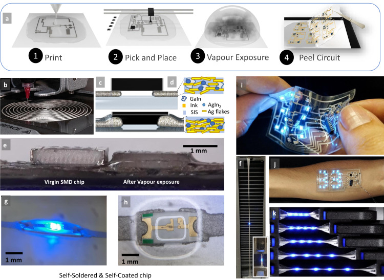
Fig. 1. Fabrication process for hybrid stretchable circuits.
a Process for chip-integrated circuit fabrication. Printing using an extrusion printer and the Ag–In–Ga–SIS ink, pick and place of microchips, Pol–Gel transition through solvent vapor exposure, and peeling of the circuit. b Example of a digitally printed circuit with 14 layers of ink. c Schematics of the chip interfacing through Pol–Gel. d Schematics of the ink microstructure before and after vapor exposure. e Side view of a small resistor chip before and after vapor exposure. f A sample with an integrated LED, after being cut, and healed through Pol–Gel, <900% strain. g Side view of a self-encapsulated circuit through Pol–Gel. h Top view of a self-encapsulated circuit through Pol–Gel. i Soft-matter circuit with integrated sensors, microprocessor, and LED display for temperature measurement. j Same circuit was applied to the skin. k Example of a circuit with multiple LEDs under strain. The authors affirm that the human research participant (first author P.L.) provided informed consent for publication of the images in (i, j).

