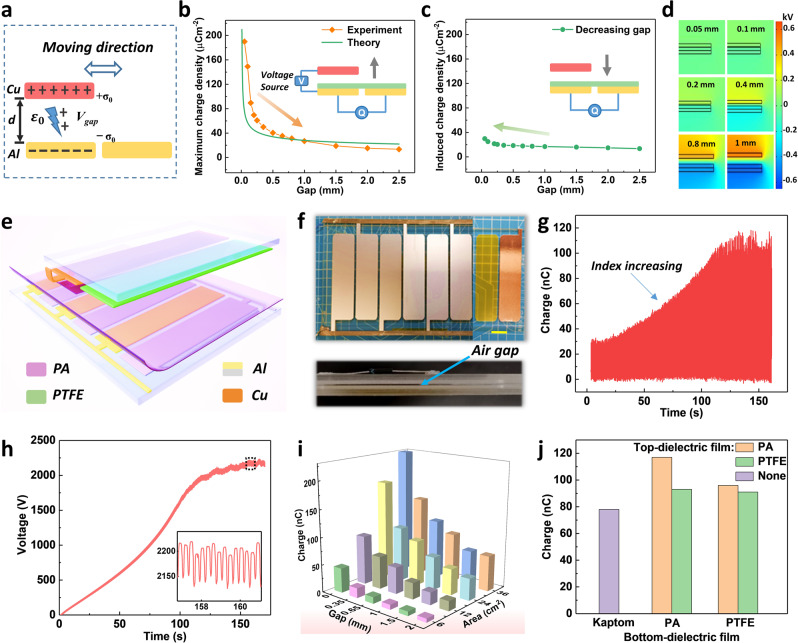
Fig. 2. The air breakdown model of non-contact TENG and the structure influence on the output of plane FSS-TENG.
a The equivalent physical model of the non-contact TENG. b The plots of experimental and theoretical maximum charge density vs. the gap for the non-contact TENG with charge excitation. The inset refers to the measurement method. c The plot of charge density vs. the gap for the non-contact TENG without charge excitation. The inset refers to the measurement method. d The simulated potential distribution of difference gaps at 10 μC m−2. e The 3D schematic of plane FSS-TENG. f Device photograph of the top view and side view. The area of each electrode and PTFE are 23.3 cm2. Scale bar: 2 cm. g The dynamic output charge accumulation process with charge self-excitation. h The dynamic excitation voltage between top and bottom electrodes. i The output charge of plane FSS-TENG with different electrode area and air gaps (the gap of 0 mm represents the full contact state); the surface of the Al electrode is attached with a 25 μm Kapton film and the Cu electrode without film. j Output charge with different materials (FEP, PTFE, and Kapton, the air gap is 0.35 mm). Driving frequency is 2 Hz for g–j.

