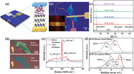
Figure 1.

Fabrication and characterizations of HfSe2 oxide films and devices. a) Schematic illustration of Ti/HfSe x O y /HfSe2/Au memristor. b) Optical image of the fabricated device. The crosspoint area is 5 × 5 µm2. The inset images show AFM scan of the crosspoint (left lower panel) and AFM height profile (left upper panel) across the white line. c) XRD patterns of the HfSe2 nanosheets on the SiO2 substrate. d) Optical microscopy images of an exfoliated HfSe2 flake with different thicknesses. The transparency of the flake increases after O2‐plasma treatment, indicating the formation of Hf—O layer. e) Room‐temperature Raman spectra before and after 5 min O2‐plasma treatment of HfSe2 using a 532 nm laser. f) XPS spectra of Hf 4f core level for air‐exposed and O2‐plasma‐treated HfSe2 flakes.
