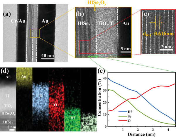
Figure 4.

a) Cross‐sectional TEM image of the device. b) Amplified HAADF image of the device structure in the selected TEM imaging of (a). c) Amplified TEM image of layered HfSe2 in (b), showing that the interlayer distance along [001] axis of the trigonal HfSe2 is 0.616 nm. d) Cross‐sectional TEM image of the Ti/HfSe x O y /HfSe2/Au heterostructure and EDS elemental mapping of Au, Ti, Hf, Se, and O. e) EDS line scan across the HfSe x O y layer, along the green arrow in (b).
