
Figure 1.
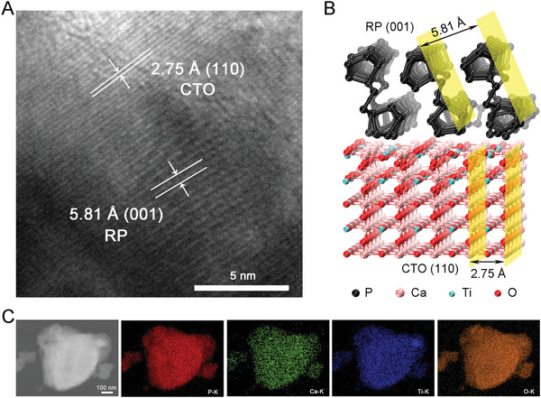
Morphology of CTO/RP P–N heterojunction. A) High‐resolution transmission electron microscopy (HRTEM) image of P–N heterointerface of CTO/RP and corresponding lattice spacing calibration of CTO and RP. Scale bar: 5 nm. B) Optimized geometric structures of CTO/RP P–N heterojunction, where black, pink, pale green, and red spheres represent P, Ca, Ti, and O atoms, respectively. The yellow plane refers to the corresponding lattice facets. C) Energy dispersive X‐ray spectroscopy (EDS) mapping of CTO/RP P–N heterojunction. (red: P; green: Ca; blue: Ti; orange: O)