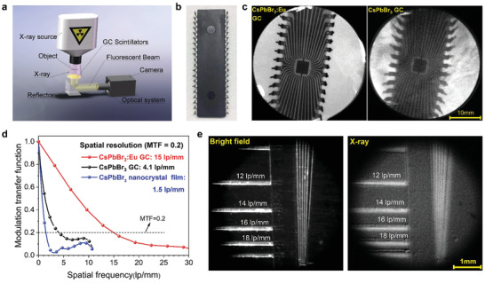
Figure 3.

Spatial resolution evaluation of X‐ray imaging based on three scintillators: CsPbBr3 nanocrystal film, CsPbBr3 GC, and CsPbBr3:1.5%Eu GC. a) The schematic of X‐ray imaging system. b) Photograph of chip A. c) X‐ray images of chip A using CsPbBr3 GC scintillators with and without Eu3+ doping (dose rate: 47.2 µGyair s−1, voltage: 50 KV). d) Modulation transfer functions (MTF) of X‐ray images obtained from CsPbBr3 GC scintillators with and without Eu3+ doping, the conventional CsPbBr3 nanocrystal film scintillator is set as reference. The image's spatial resolutions (when MTF value equals 0.2) acquired from CsPbBr3 GC, CsPbBr3:Eu GC, and CsPbBr3 QDs scintillators are 15.0, 4.1, and 1.5 lp mm−1, respectively. e) Bright field and X‐ray image of standard X‐ray resolution test pattern plate using CsPbBr3:Eu GC scintillator (dose rate: 189 µGyair s−1, voltage: 50 KV).
