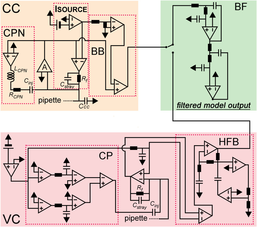
Figure 1.
Model amplifier. Schematic circuit diagram of the model amplifier. The current clamp circuit (CC) consisted of a current source (ISOURCE), an idealized voltage buffer (A), capacitance neutralization (CPN), and bridge balance (BB) circuits. The voltage clamp circuit (VC) consisted of a resistive feedback amplifier with dual capacitance compensation (CP) and the high-frequency boost circuit (HFB). Outputs of the two amplifier modules are connected to a low-pass filter circuit (BF). The test configurations used to characterize the implemented amplifier components are shown in Extended Data Figure 1-1.

