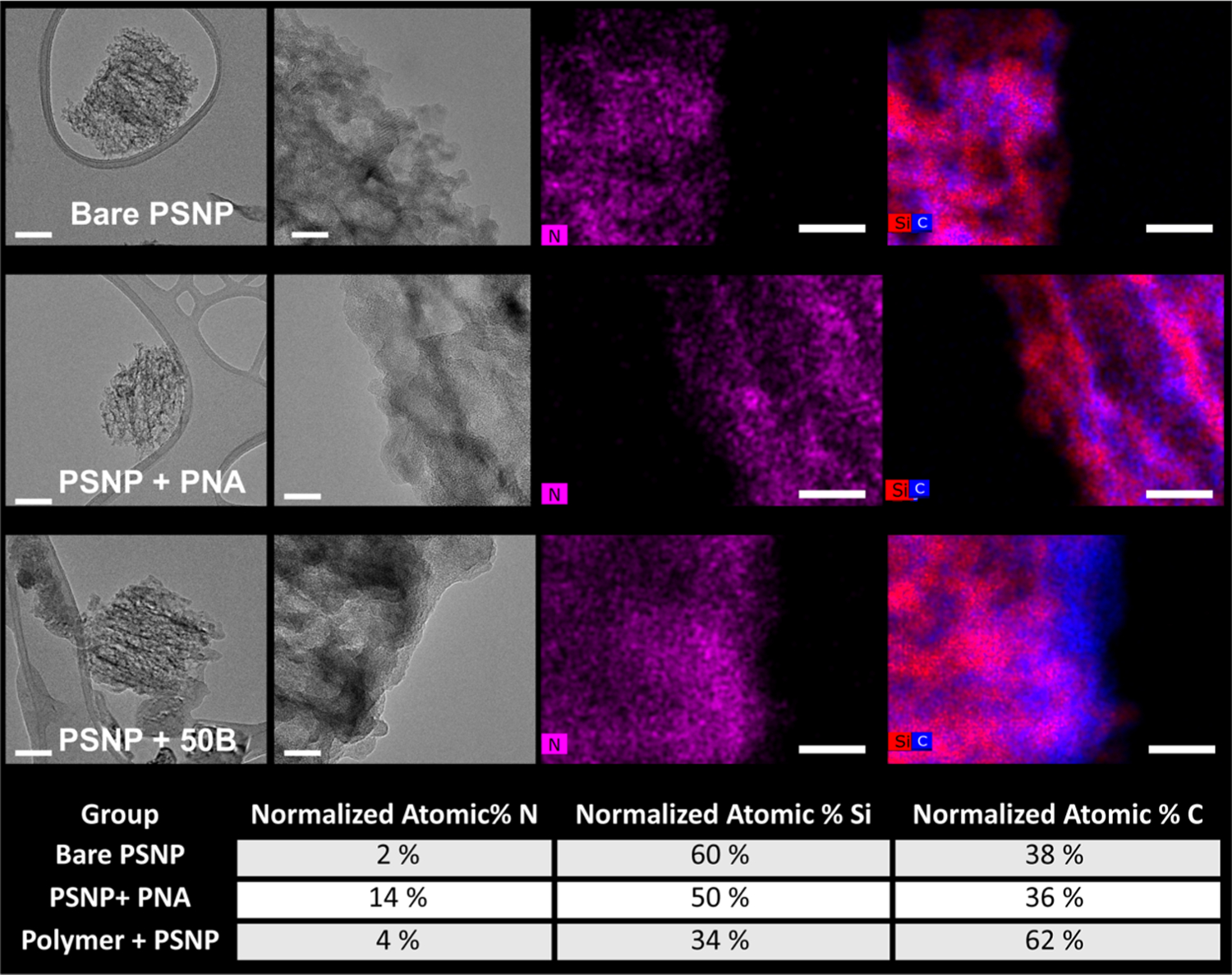
Figure 3.

TEM panel shows representative images for bare PSNPs, PNA-loaded PSNPs, and polymer-coated PSNPs. TEM and EDS data for all composites are provided in Figure S5A,B. From left to right, the images depict an individual particle, a high-resolution image of the particle edge, nitrogen map (PNA loading), and a silicon–carbon map (polymer coating). Scale bar = 100 nm for the TEM image on the left and 20 nm for the three images on the right. Note that the microscopy software used automatically scales each image to a similar brightness intensity, so the relative elemental composition between groups cannot be inferred from image visualization alone. The table at the bottom of the figure shows quantification of the normalized atomic % for each element from the EDS analysis.
