
Figure 3.
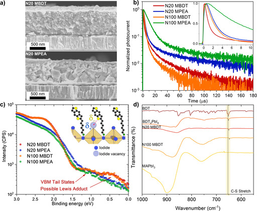
(a) Cross‐sectional SEM images of N20 MBDT(top) and N20 MPEA layers solution‐processed onto FTO substrates and capped with an Au overlayer (to facilitate measurement). (b) Normalized device photocurrent as a function of time after a 5 ns pulse (550 nm wavelength) shown in the log scale over the long‐time frame and a linear scale for the short time regime (inset). (c) UV photoelectron spectroscopy measurements of the perovskite thin films deposited on FTO substrates. The inset shows a schematic of hypothesized undercoordinated Pb passivation via –S (thiophene) Lewis adduct formation (d) ATR‐FTIR data for a BDT drop cast film, BDT2PbI4, N20 MBDT, N100 MBDT and MAPbI3 reference thin films with a highlight of the C−S stretch peak shift, the asterisks represent the peak positions.