

Freestanding membranes of electronically reconfigurable complex oxide heterostructure are demonstrated.
Abstract
In recent years, lanthanum aluminate/strontium titanate (LAO/STO) heterointerfaces have been used to create a growing family of nanoelectronic devices based on nanoscale control of LAO/STO metal-to-insulator transition. The properties of these devices are wide-ranging, but they are restricted by nature of the underlying thick STO substrate. Here, single-crystal freestanding membranes based on LAO/STO heterostructures were fabricated, which can be directly integrated with other materials via van der Waals stacking. The key properties of LAO/STO are preserved when LAO/STO membranes are formed. Conductive atomic force microscope lithography is shown to successfully create reversible patterns of nanoscale conducting regions, which survive to millikelvin temperatures. The ability to form reconfigurable conducting nanostructures on LAO/STO membranes opens opportunities to integrate a variety of nanoelectronics with silicon-based architectures and flexible, magnetic, or superconducting materials.
INTRODUCTION
Complex oxide heterostructures exhibit diverse emergent properties, including a tunable metal-to-insulator transition (1), magnetism (2), superconductivity (3, 4), inhomogeneous transport (5), and spin-orbit coupling (6, 7). In particular, the ability to electronically control the conductivity of the LaAlO3/SrTiO3 (LAO/STO) interface with conductive atomic force microscopy (c-AFM) lithography opens opportunities to create various electronic structures such as single-electron transistors (8), electron waveguides (9), and photon detectors (10). In addition to providing new avenues for technological application, these devices allow us to reveal fundamental behavior characteristic of correlated electronic systems (11–13). Furthermore, there are huge potential of LAO/STO heterostructure unleashed when its functionality can be integrated with other materials.
Previously, options for integrating LAO/STO with other materials have been restricted to what is directly placed on top of the LAO surface. By integrating graphene on top of LAO/STO, it has been shown that the charge neutrality point of graphene can be locally and dynamically controlled with nanoscale precision (14). However, the c-AFM technique, which is based on the protonation of LAO surface to attract electrons to the interface (15, 16), limits the material on top of LAO/STO to be so thin that protons can penetrate through. For example, LAO/STO cannot be patterned with c-AFM lithography if bilayer or multilayer graphene is placed on the top (17). Another approach for integrating LAO/STO heterostructures is to grow LAO/STO directly on the top of other materials. However, there are strict limitations on substrate material selection since heteroepitaxy requires very similar lattice constants and crystal structures (18). Besides, it is well known that formation of a two-dimensional electron gas (2DEG) is very sensitive to point defects and the strain state of STO (19, 20). The ability of c-AFM lithography to create nanostructures in LAO/STO depends sensitively on the quality of the underlying STO. Conductive nanostructures, previously created with molecular beam epitaxy–grown LAO/STO on Si substrate, have a relatively large sheet resistance, which is likely related to structural defects in the STO layer that is due to the lattice mismatch between STO and Si (21).
A promising approach for integration of LAO/STO is to create a freestanding ultrathin (submicrometer) layer that can be integrated with other materials similar to the way in which van der Waals stacks are produced with 2D layered materials such as graphene, hexagonal boron nitride, and transition metal dichalchogenides (22). To create these freestanding materials, it is desirable to start with an established thin-film growth technique, followed by a strategy for releasing the top layer from the substrate. Synthesis and transfer of several perovskite oxides and oxide heterostructures have been previously realized with the help of a Sr3Al2O6 sacrificial layer (23–25). Note that although Sr3Al2O6 surface enables preserving the perovskite step and terrace structure of the underlying substrate, the termination control may not be easily achieved (20, 26). The LAO/STO membrane can also be realized by strain engineering (27), but the size of a single piece is limited to several micrometers, and the thickness of STO layer cannot be controlled. Besides, this method requires the LAO layer to be tens of nanometers in thickness, which will lead to metallic state of LAO/STO interfaces, indicating that c-AFM lithography is incompatible.
To realize a transferrable and reconfigurable LAO/STO-based 2DEG, three properties need to be preserved: (i) tunable metal-to-insulator transition, (ii) conductance comparable to that of typical LAO/STO 2DEG, and (iii) persistence of conductivity to cryogenic temperatures. Here, we demonstrate how to create freestanding LAO/STO membranes that meet all three requirements. The transferred freestanding membrane preserves its single-crystalline structure and atomically smooth surface. Nanoscale conducting regions at the heterointerface can be created and erased by c-AFM lithography. The conductive nanowire we sketched on the sample survives at cryogenic temperature and shows possible superconducting behavior. We also discuss some future directions opened up by the newly developed LAO/STO membrane platform.
RESULTS
Fabrication of freestanding LAO/STO membrane
To develop freestanding form of LAO/STO, careful consideration of lattice symmetry, growth thermodynamics, and etchant selectivity for the sacrificial layer and membrane material is required. Our approach to releasing LAO/STO from its oxide substrate here is to insert a sacrificial SrRuO3 (SRO) layer between pulsed laser deposition (PLD)–grown LAO/STO film and oxide substrates (28). Since the heterointerface property of LAO/STO highly depends on the quality of STO, synthesizing high-quality STO/SRO templates is crucial for this study. It requires not only minimizing point defect formation but also creating an atomically flat surface with TiO2 termination. A schematic of LAO/STO freestanding membrane fabrication process is shown in Fig. 1A. We first grew a SRO (20-nm) epitaxial layer followed by a 200-nm-thick STO layer on a STO (001) substrate by PLD. The thicknesses of the SRO and STO layers were controlled by monitoring reflection high-energy electron diffraction (RHEED) oscillations (Fig. 1B). Next, we implemented buffered hydrofluoric acid (BHF) etching and annealing to make the STO surface TiO2-terminated. Figure 1C shows the 2θ x-ray diffraction (XRD) patterns of a STO/SRO template. Since reflections of STO substrate and film are not distinguishable, we conclude that cation stoichiometry in the PLD-grown STO is close to ideal (red curve in fig. S2) (29). The AFM topography shows an atomically flat surface with 3.9-Å unit cell (u.c.) steps (Fig. 1F), which is consistent with the STO substrate u.c. height. Then, a 10-u.c.-thick LAO film was deposited on the top of STO/SRO template. The LAO/STO heterostructure was released from the substrate by selective etching of the sacrificial SRO layer in an aqueous solution of NaIO4. After the SRO was selectively etched, the released LAO/STO film floated on the solution. An Al2O3 substrate was then used to catch the freestanding LAO/STO film. Figure 2A shows an optical image of a millimeter-sized LAO/STO membrane transferred onto Al2O3 (0001) substrate. The LAO (002), STO (002), and Al2O3 (0006) peaks are all clearly observed in the 2θ – ω x-ray scan, indicating that the LAO/STO membrane preserves its single-crystalline phase after the transfer (Fig. 2B). The AFM scan of LAO/STO film confirms its atomically flat surface (Fig. 2C). Scanning transmission electron microscopy high-angle annular dark field (STEM-HAADF) and atomic-resolution energy dispersive spectroscopy (EDS) investigations were performed on LAO/STO/Al2O3 heterostructure to examine the interfacial atomic structure. The STEM-HAADF image shows that the LAO/STO interface is dislocation-free, which means that the epitaxial LAO/STO flake has a relatively high crystal quality (fig. S1). The EDS maps show that the chemically abrupt interface consists of LAO and layer of STO as we designed (Fig. 2E).
Fig. 1. STO/SRO template growth.
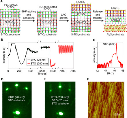
(A) Process schematic for oxide growth, membrane release, and transfer. (B) In situ RHEED intensity oscillation during the PLD deposition of SRO and STO films. a.u., arbitrary units. (C) Out-of-plane 2θ − ω XRD patterns of STO/SRO grown on STO (001) substrate around (002) STO peak. (D and E) RHEED patterns at each step of the PLD growth. (F) AFM images measured on the surface of STO/SRO grown on STO (001) substrate.
Fig. 2. Characteristics of freestanding LAO/STO membrane.
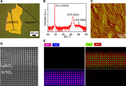
(A) Optical microscope image of a LAO (10 u.c.)/STO (200 nm) freestanding membrane transferred onto sapphire substrate. (B) XRD 2θ − ω scan of a LAO (10 u.c.)/STO (200 nm) freestanding membrane transferred onto sapphire substrate. (C) AFM image of a LAO (10 u.c.)/STO (200 nm) freestanding membrane transferred onto sapphire substrate. (D) STEM-HAADF image obtained at the LAO/STO interface. (E) EDS elemental mapping of the LAO/STO interface. The interface is atomically abrupt, and intermixing is not notable.
Electrical tunability of 2DEG with c-AFM lithography
The electrical tunability of the transferred membrane is investigated via c-AFM lithographic patterning. Electrical contact to the LAO/STO interface was fabricated using Ar+ milling, followed by sputter deposition of Ti/Au; a second layer of Ti/Au on top was added for wire bonding (see Materials and Methods). Figure 3A shows an optical microscope image of the membrane after electrodes deposition, where a micrometer-sized area is surrounded by interface electrodes to form c-AFM lithography canvas (Fig. 3B). We found that the as-transferred LAO (10 u.c.)/STO (200 nm) heterostructure shows insulating behavior with gigohm (see note S1). Note that our target was an insulating LAO/STO interface that could be programmed using c-AFM lithography. The c-AFM lithography setup is represented in Fig. 3C with pattern of a four-terminal nanowire. As shown in Fig. 3B, the tip first sketches green triangular regions in with Vtip=8 V, followed by sketching of the main channel (yellow path with length L = 1.4 μm) with Vtip=6 V. During c-AFM lithography, we source voltage V1 = Vpp cos (2πft) (where t is time; peak-to-peak voltage Vpp = 200 mV; frequency f = 9 Hz) from electrode 1 and performed lock-in measurement of current I14 through electrode 4 and the voltage V82 across electrode pairs 8 and 2 (Fig. 3C). Thus, four-terminal conductance can be determined by G4T = I14/V82. Once the main channel is completed, a sharp conductance jump around 2 μS can be detected, indicating the creation of conducting region at LAO/STO interface (Fig. 3D). The voltage threshold for forming conducting channels is around Vtip=3 V. This process is reversible: When the tip is negatively biased (Vtip=−2 V) and sketched across the existing wire along the red path in Fig. 3B, a steep drop in the conductance is observed (Fig. 3D). The width of the wire can be determined by fitting the conductance drop using the function (30)
where a1−3 are fitting parameters, x = vt is the position of the tip moving at velocity v, x0 represents the center position of the wire, and W is the width of the wire (fig. S4A). The sheet resistance Rs can be calculated by Rs = W/(G4TL). The wire width and sheet resistance extracted from nanowires created with different positive voltages are shown in fig. S4B. Larger positive bias on the tip yields nanowire with lower sheet resistance, indicating that more electrons are attracted to the interface, while the width of the wire ranges between 15 and 20 nm without a clear monotonic dependence on the writing voltage. These values are close to c-AFM–patterned nanowires at LAO/bulk STO interface (see note S3).
Fig. 3. Creating and cutting conducting wires at the LAO/STO membrane interface.
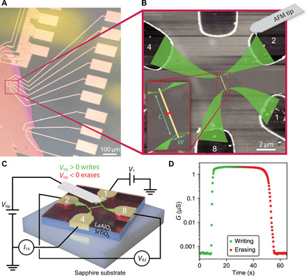
(A) Optical microscope image of the freestanding LAO (10 u.c.)/STO (200 nm) membrane after depositing electrodes to make the c-AFM lithography canvases. (B) AFM image of a canvas overlaid by a designed c-AFM lithography pattern. The green region is made conducting by c-AFM lithography to serve as an extension of gold electrodes. The yellow line is a nanowire that has length L = 1.4 μm. After writing the nanowire with positive bias, the AFM tip sketches along the red line with negative bias to cut the previous nanowire. (C) Schematic drawing of c-AFM lithography. Gold electrodes are in contact with LAO/STO interface. Green wires indicate the nanoscale conducting regions at the interface created by positively biased AFM tip sketching on the LAO surface. Sketching with a negative bias on the tip will restore the insulating phase at the interface. (D) Four-terminal conductance increases more than three orders of magnitude after the tip finishes sketching the main channel with +6-V tip bias. Then, the conductance is restored to close to 0 nS by sketching across the main channel with −2-V tip bias.
Low-temperature electrical properties of c-AFM–patterned nanowires
To investigate the low-temperature electrical properties of LAO/STO membrane, we performed transport measurements on three different devices at millikelvin temperatures. Here, we describe the result obtained for device C. The results for device A and device B are shown in fig. S7. Before writing the device, the canvas is switched to a fully insulating phase by scanning the entire canvas with a negative voltage, both horizontally and vertically with 10-nm line spacing. To compensate the fast decay of the conducting channels during the transfer to fridge (see note S4), robust 2D virtual leads extending from gold leads to the middle of the canvas are first made with 50-nm line spacing (Fig. 4A). A zoom-in view of these virtual leads is shown in fig. S5A. Then, the 1.2-μm-long nanowire is created, which yields a four-terminal conductance jump of 3 μS at room temperature (fig. S5B). During cryogenic measurements, we source voltage V1 from electrode 1 while measuring current I14 through electrode 4 and voltage V85 across electrode pairs 8 and 5. Figure S5C shows the temperature dependence of the two-terminal and four-terminal conductance of the nanowire, both of which exhibit metallic behavior from room temperature down to 34 K and localization behavior from 34 to 1 K, which results from carrier freezing at low temperature (31). The two-terminal conductance begins to increase as the temperature is lowered from 300 mK.
Fig. 4. Superconductivity in a nanowire created at the LAO/STO membrane interface (device C).
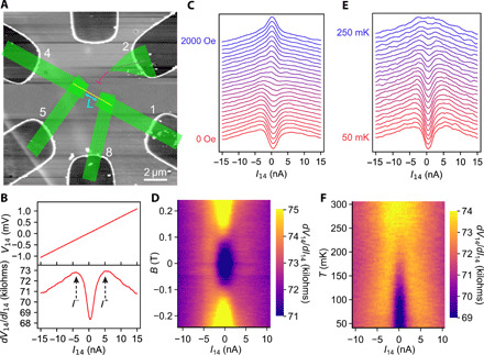
(A) AFM image of the canvas overlaid by a designed c-AFM lithography pattern. The green region is made conducting by c-AFM lithography to serve as an extension of gold electrodes. The yellow line is the main channel with length L = 1.2 μm. (B) Two-terminal I-V curve (top) acquired at 0 T and 50 mK and the corresponding differential resistance curve dV/dI curve (bottom) show a superconducting feature. The critical current is Ic = 4.9 nA. (C) dV/dI curves at 80 mK with increasing out-of-plane magnetic field through the superconducting transition. (D) dV/dI intensity map as a function of magnetic field and bias current. (E) Temperature-dependent dV/dI curves at 0 T. (F) dV/dI intensity map as a function of temperature and bias current.
At 50-mK base temperature and zero magnetic field, nonlinearity is observed in two-terminal I-V curve at small current value, where the differential resistance dV/dI is lower (Fig. 4B). We attribute this feature to a superconducting region located somewhere between current source and drain. The critical current is calculated from the average of the two resistance peaks Ic = (I+ + I−)/2 = 4.9 nA. The dip in dV/dI curve disappears at elevated temperature or magnetic fields. Figure 4C shows the differential resistance calculated from I-V curves acquired at T = 80 mK and under different magnetic fields over the range ∣B∣≤0.2 T. Each curve is shifted by ΔR=0.8 kilohms for clarity. As the magnetic field passes beyond the upper critical field, Ic gradually decreases, while the differential resistance near zero bias increases. Figure 4D shows an intensity plot of the differential resistance as a function of magnetic field and bias current. The signal is symmetric with respect to magnetic field, and the upper critical field for this device is Bc2=0.1 T. Similarly, Fig. 4E shows the differential resistance calculated from I-V curves measured at zero magnetic field while varying temperature from T=50 to 300 mK with ΔT= 5-mK step. The suppression of the superconducting feature is also observed with a critical temperature near T=200 mK, which can be inferred from the intensity plot of temperature and bias current (Fig. 4F). The critical temperature and critical field observed for this device at LAO/STO membrane interface are consistent with superconductivity observed in LAO/STO nanowires (32, 33).
However, as shown in fig. S6A, the corresponding four-terminal I-V measurements are not showing a reduced differential resistance near zero bias. One possible explanation is that the superconducting region is located outside the main channel, in the virtual leads rasterized by the AFM tip rather than in the main channel, while the electron density in the main channel falls outside the bounds for superconductivity. In another device (A), however, the superconductivity results in zero bias dip in both two-terminal and four-terminal dV/dI curve (fig. S7B). For device C, at magnetic field larger than 1 T, both the two-terminal resistance and four-terminal resistance decrease with increasing field (fig. S6B). This negative magnetic resistance is possibly caused by the detrapping of frozen-out carriers by magnetic field (31).
DISCUSSION
This transport results demonstrate that the use of chemical release method to realize the freestanding form of LAO/STO heterostructure preserves the integrity of the LAO/STO. Highly reconfigurable nanostructure on LAO/STO membrane with dimensions comparable to current semiconductor technology components can be created by c-AFM lithography.
Looking forward, the fact that conductive nanowires survive at dilution fridge temperatures holds great promise for this freestanding 2DEG platform to realize emergent properties and functionalities upon integration with variety of other materials (Fig. 5A). Removing the STO substrate can enable sizeable strains to be applied, which may not only substantial alter the electronic and superconducting properties but also provide interesting electromechanical interactions. LAO/STO-based flexible nanoelectronics can also be developed (Fig. 5B). LAO/STO nanostructures can also serve as metallic gates that can create quantum confinement, modulate exchange interactions, and otherwise mediate electrostatic interactions in other 2D layers and near-surface materials, including silicon. For example, upon integrating with Si/SiGe, LAO/STO 2DEG can serve as the top gates to confine quantum dots, and because of the versatile control of c-AFM lithography, the location of the quantum dots can be easily redefined (Fig. 5C). Putting LAO/STO 2DEG on other functional oxides or low-dimensional materials may result in a new generation of reconfigurable photonic detectors and tunneling junctions (Fig. 5D). On the other hand, it would be interesting to investigate how the strongly correlated LAO/STO 2DEG would behave in the proximity of magnets, other superconductors, and topological insulators. For instance, if we put LAO/STO membrane on top of ferromagnets such as NiFe, then we can pump spin current into LAO/STO interface and study the spin-orbit coupling in c-AFM–defined nanodevices, instead of growing NiFe on top of LAO (34). Furthermore, LAO/STO membrane gets rid of bulk STO substrate that has large dielectric loss tangent, making it a possible platform for microwave resonators and waveguides (Fig. 5E) (35).
Fig. 5. Possible integration motifs for LAO/STO membranes.
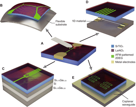
(A) LAO/STO reconfigurable 2DEG platform. (B) LAO/STO integrated with flexible materials to achieve flexible electronics. (C) LAO/STO 2DEG can be used to confine silicon quantum dots. (D) LAO/STO 2DEG can serve as gate for 1D or 2D materials. (E) AFM-patterned LAO/STO resonators coupled to a microwave waveguide.
MATERIALS AND METHODS
Epitaxial film fabrication
SRO, STO, and LAO thin films were epitaxially grown on TiO2-terminated STO substrates using PLD with in situ RHEED monitoring. To achieve the TiO2-terminated substrates, as-received STO substrates were etched by buffered hydrofluoric acid (HF) for 1 min and annealed at 1000°C for 6 hours. During the SRO and STO film growth, the temperature of the PLD chamber was kept as 615° and 750°C, respectively. The oxygen partial pressure was 0.12 and 0.1 mbar, respectively. After growing STO/SRO, the samples were cooled down to room temperature under an oxygen ambient of 1 atm. To obtain the TiO2-terminated STO/SRO template, STO/SRO film grown on STO substrate was etched by buffered HF for 10 s and annealed at 900°C for 2 hours. The atomically flat surface on the thermally treated substrate is shown by atomic for microscopy images in Fig. 1F. LAO film was then grown in an ambient oxygen pressure of 1 × 10⁻³ mbar with substrate temperature of 550°C and was cooled down to room temperature under an oxygen ambient of 1 atm.
Release of freestanding membranes
The oxide heterostructure was immersed into a 0.4-mol NaIO4 solution to dissolve the SRO layers at room temperature. After 48 hours, LAO/STO film was released and collected from solution. Then, the film was washed by deionized water and picked up by Al2O3 substrate.
Patterning of electrodes
LAO/STO membrane samples were patterned with a maskless laser aligner (Heidelberg, MLA100) using AZ4110 photoresist. After exposure and developing, the sample underwent ion milling 29 nm and backfilling with 4-nm titanium and 25-nm gold in a Plassys 8 pocket e-Gun evaporator with built-in ion gun. Excessive metals were lifted off in acetone. Then, the bonding pads were deposited with 5-nm titanium and 27-nm gold at a small angle, which were able to cover the edge of LAO/STO membrane.
c-AFM lithography
The c-AFM lithography was carried out in an Asylum Research MFP-3D AFM under conditions of controlled relative humidity (40%) and temperature (293 K). The interface of LAO/STO membrane was grounded during writing, and the DC writing voltage was applied to c-AFM tip through a 100-kilohm resistor.
Low-temperature transport measurement
Low-temperature transport measurements were performed in a Quantum Design Physical Property Measurement System (PPMS) dilution refrigerator. Source voltages were applied by a 24-bit digital/analog converter National Instruments PXI-4461, which can also simultaneously perform 24-bit analog/digital conversion. The drain current was measured after amplification by a subfemtoampere current amplifier (Femto DDPCA300). The four-terminal voltage drop was measured by a differential voltage amplifier (Femto DLPVA), which has 1-terohm input impedance.
STEM characterization
The atomic structure imaging was conducted on LAO/STO/Al2O3 sample by using Cs-corrected TEM (JEOL-ARM300F) operated at 300 kV. Convergence angle for both STEM and EDS acquisition was 35.63 mrad. Collection angle for HAADF imaging was 68 to 280 mrad. Energy-dispersive x-ray spectrometer with a detectable area of 100 mm2 was used in STEM imaging mode. EDS maps with a total number of 3020 frames were acquired with a speed of 0.655 s per frame with 256 by 256 pixels. The specimen drift was corrected during acquisition. Each elemental map is constructed by integrating the signal from La-Lα, Sr-Lα, Al-Kα, and Ti-Kα characteristic x-rays, respectively. The EDS maps in Fig. 2 were processed by the Wiener filter to minimize random noise, and the averaged EDS profiles in fig. S1 were obtained from the maps without filtering, which do not contain artifact from filtering.
Acknowledgments
Funding: This research is funded by the Gordon and Betty Moore Foundation’s EPiQS Initiative, grant GBMF9065 to C.-B.E., Vannevar Bush Faculty Fellowship (N00014-20-1-2844 (C.-B.E.), N00014-15-1-2847 (J.L.)), AFOSR (FA9550-15-1-0334 (C.-B.E.)), NSF through the University of Wisconsin MRSEC (DMR-1720415), PHY-1913034 (J.L.), ONR N00014-20-1-2481 (J.L.), and ONR MURI (N00014-21-1-2537) (J.L., C.-B.E.). Transport measurement at the University of Wisconsin–Madison was supported by the US Department of Energy (DOE), Office of Science, Office of Basic Energy Sciences (BES), under award number DE-FG02-06ER46327. The STEM work at SKKU was supported by the Samsung Research Funding and Incubation Center of Samsung Electronics under project number SRFC-MA1702-01 (to S.H.O.). Author contributions: C.-B.E., J.L., K.E., and M.Y. conceived the research. C.-B.E. and J.L. supervised the experiments. K.E., J.-W.L., and H.L. performed the sample growth and membrane fabrications. M.Y., D.Y., and P.I. performed the device fabrication, c-AFM lithography, and transport measurements at low temperature. J.S. and S.H.O. carried out STEM measurements. K.E., M.Y., J.L., and C.-B.E. wrote the manuscript. All authors discussed the results and commented on the manuscript. C.-B.E. directed the research. Competing interests: The authors declare that they have no competing interests. Data and materials availability: All data needed to evaluate the conclusions in the paper are present in the paper and/or the Supplementary Materials. Data necessary to understand and evaluate the conclusions of this paper are archived at https://doi.org/10.7910/DVN/QGZ0NM. Additional data related to this paper may be requested from the authors.
SUPPLEMENTARY MATERIALS
Supplementary material for this article is available at http://advances.sciencemag.org/cgi/content/full/7/33/eabh1284/DC1
REFERENCES AND NOTES
- 1.Thiel S., Hammerl G., Schmehl A., Schneider C. W., Mannhart J., Tunable quasi-two-dimensional electron gases in oxide heterostructures. Science 313, 1942–1945 (2006). [DOI] [PubMed] [Google Scholar]
- 2.Brinkman A., Huijben M., Van Zalk M., Huijben J., Zeitler U., Maan J. C., Van der Wiel W. G., Rijnders G., Blank D. H. A., Hilgenkamp H., Magnetic effects at the interface between non-magnetic oxides. Nat. Mater. 6, 493–496 (2007). [DOI] [PubMed] [Google Scholar]
- 3.Reyren N., Thiel S., Caviglia A. D., Kourkoutis L. F., Hammerl G., Richter C., Schneider C. W., Kopp T., Ruetschi A. S., Jaccard D., Gabay M., Muller D. A., Triscone J. M., Mannhart J., Superconducting interfaces between insulating oxides. Science 317, 1196–1199 (2007). [DOI] [PubMed] [Google Scholar]
- 4.Caviglia A. D., Gariglio S., Reyren N., Jaccard D., Schneider T., Gabay M., Thiel S., Hammerl G., Mannhart J., Triscone J. M., Electric field control of the LaAlO3/SrTiO3 interface ground state. Nature 456, 624–627 (2008). [DOI] [PubMed] [Google Scholar]
- 5.Kalisky B., Spanton E. M., Noad H., Kirtley J. R., Nowack K. C., Bell C., Sato H. K., Hosoda M., Xie Y., Hikita Y., Woltmann C., Pfanzelt G., Jany R., Richter C., Hwang H. Y., Mannhart J., Moler K. A., Locally enhanced conductivity due to the tetragonal domain structure in LaAlO3/SrTiO3 heterointerfaces. Nat. Mater. 12, 1091–1095 (2013). [DOI] [PubMed] [Google Scholar]
- 6.Caviglia A. D., Gabay M., Gariglio S., Reyren N., Cancellieri C., Triscone J. M., Tunable Rashba spin-orbit interaction at oxide interfaces. Phys. Rev. Lett. 104, 126803 (2010). [DOI] [PubMed] [Google Scholar]
- 7.Shalom M. B., Sachs M., Rakhmilevitch D., Palevski A., Dagan Y., Tuning spin-orbit coupling and superconductivity at the SrTiO3/LaAlO3 interface: A magnetotransport study. Phys. Rev. Lett. 104, 126802 (2010). [DOI] [PubMed] [Google Scholar]
- 8.Cheng G., Siles P. F., Bi F., Cen C., Bogorin D. F., Bark C. W., Folkman C. M., Park J. W., Eom C. B., Medeiros-Ribeiro G., Levy J., Sketched oxide single-electron transistor. Nat. Nanotechnol. 6, 343–347 (2011). [DOI] [PubMed] [Google Scholar]
- 9.Tomczyk M., Cheng G., Lee H., Lu S., Annadi A., Veazey J. P., Huang M., Irvin P., Ryu S., Eom C.-B., Levy J., Micrometer-scale ballistic transport of electron pairs in LaAlO3/SrTiO3 nanowires. Phys. Rev. Lett. 117, 096801 (2016). [DOI] [PubMed] [Google Scholar]
- 10.Irvin P., Ma Y., Bogorin D. F., Cen C., Bark C. W., Folkman C. M., Eom C.-B., Levy J., Rewritable nanoscale oxide photodetector. Nat. Photonics 4, 849–852 (2010). [Google Scholar]
- 11.Cheng G., Tomczyk M., Lu S., Veazey J. P., Huang M., Irvin P., Ryu S., Lee H., Eom C. B., Hellberg C. S., Levy J., Electron pairing without superconductivity. Nature 521, 196–199 (2015). [DOI] [PubMed] [Google Scholar]
- 12.Annadi A., Cheng G., Lee H., Lee J.-W., Lu S., Tylan-Tyler A., Briggeman M., Tomczyk M., Huang M., Pekker D., Eom C.-B., Irvin P., Levy J., Quantized ballistic transport of electrons and electron pairs in LaAlO3/SrTiO3 Nanowires. Nano Lett. 18, 4473–4481 (2018). [DOI] [PubMed] [Google Scholar]
- 13.Briggeman M., Tomczyk M., Tian B., Lee H., Lee J.-W., He Y., Tylan-Tyler A., Huang M., Eom C.-B., Pekker D., Mong R. S. K., Irvin P., Levy J., Pascal conductance series in ballistic one-dimensional LaAlO3/SrTiO3 channels. Science 367, 769–772 (2020). [DOI] [PubMed] [Google Scholar]
- 14.Li J., Guo Q., Chen L., Hao S., Hu Y., Hsu J.-F., Lee H., Lee J.-W., Eom C.-B., D’Urso B., Irvin P., Levy J., Reconfigurable edge-state engineering in graphene using LaAlO3/SrTiO3 nanostructures. Appl. Phys. Lett. 114, 123103 (2019). [Google Scholar]
- 15.Bi F., Bogorin D. F., Cen C., Bark C. W., Park J. W., Eom C. B., Levy J., “Water-cycle” mechanism for writing and erasing nanostructures at the LaAlO3/SrTiO3 interface. Appl. Phys. Lett. 97, 173110 (2010). [Google Scholar]
- 16.Brown K. A., He S., Eichelsdoerfer D. J., Huang M., Levy I., Lee H., Ryu S., Irvin P., Mendez-Arroyo J., Eom C.-B., Mirkin C. A., Levy J., Giant conductivity switching of LaAlO3/SrTiO3 heterointerfaces governed by surface protonation. Nat. Commun. 7, 10681 (2016). [DOI] [PMC free article] [PubMed] [Google Scholar]
- 17.Huang M., Jnawali G., Hsu J.-F., Dhingra S., Lee H., Ryu S., Bi F., Ghahari F., Ravichandran J., Chen L., Kim P., Eom C.-B., D’Urso B., Irvin P., Levy J., Electric field effects in graphene/LaAlO3/SrTiO3 heterostructures and nanostructures. APL Mater. 3, 062502 (2015). [Google Scholar]
- 18.Chambers S. A., Epitaxial growth and properties of doped transition metal and complex oxide films. Adv. Mater. 22, 219–248 (2010). [DOI] [PubMed] [Google Scholar]
- 19.Bark C. W., Felker D. A., Wang Y., Zhang Y., Jang H. W., Folkman C. M., Park J. W., Baek S. H., Zhou H., Fong D. D., Pan X. Q., Tsymbal E. Y., Rzchowski M. S., Eom C. B., Tailoring a two-dimensional electron gas at the LaAlO3/SrTiO3 (001) interface by epitaxial strain. Proc. Natl. Acad. Sci. U.S.A. 108, 4720–4724 (2011). [Google Scholar]
- 20.Gunkel F., Wicklein S., Hoffmann-Eifert S., Meuffels P., Brinks P., Huijben M., Rijnders G., Waser R., Dittmann R., Transport limits in defect-engineered LaAlO3/SrTiO3 bilayers. Nanoscale 7, 1013–1022 (2015). [DOI] [PubMed] [Google Scholar]
- 21.Park J. W., Bogorin D. F., Cen C., Felker D. A., Zhang Y., Nelson C. T., Bark C. W., Folkman C. M., Pan X. Q., Rzchowski M. S., Levy J., Eom C. B., Creation of a two-dimensional electron gas at an oxide interface on silicon. Nat. Commun. 1, 94 (2010). [DOI] [PubMed] [Google Scholar]
- 22.Liu Y., Huang Y., Duan X., Van der Waals integration before and beyond two-dimensional materials. Nature 567, 323–333 (2019). [DOI] [PubMed] [Google Scholar]
- 23.Lu D., Baek D. J., Hong S. S., Kourkoutis L. F., Hikita Y., Hwang H. Y., Synthesis of freestanding single-crystal perovskite films and heterostructures by etching of sacrificial water-soluble layers. Nat. Mater. 15, 1255–1260 (2016). [DOI] [PubMed] [Google Scholar]
- 24.Lu D., Crossley S., Xu R., Hikita Y., Hwang H. Y., Freestanding oxide ferroelectric tunnel junction memories transferred onto silicon. Nano Lett. 19, 3999–4003 (2019). [DOI] [PubMed] [Google Scholar]
- 25.Ji D., Cai S., Paudel T. R., Sun H., Zhang C., Han L., Wei Y., Zang Y., Gu M., Zhang Y., Gao W., Huyan H., Guo W., Wu D., Gu Z., Tsymbal E. Y., Wang P., Nie Y., Pan X., Freestanding crystalline oxide perovskites down to the monolayer limit. Nature 570, 87–90 (2019). [DOI] [PubMed] [Google Scholar]
- 26.Sun H. Y., Zhang C. C., Song J. M., Gu J. H., Zhang T. W., Zang Y. P., Li Y. F., Gu Z. B., Wang P., Nie Y. F., Epitaxial optimization of atomically smooth Sr3Al2O6 for freestanding perovskite films by molecular beam epitaxy. Thin Solid Films 697, 137815 (2020). [Google Scholar]
- 27.Sambri A., Scuderi M., Guarino A., Gennaro E. D., Erlandsen R., Dahm R. T., Bjørlig A. V., Christensen D. V., Capua R. D., Ventura B. D., de Uccio U. S., Mirabella S., Nicotra G., Spinella C., Jespersen T. S., Granozio F. M., Self-formed, conducting LaAlO3/SrTiO3 Micro-membranes. Adv. Funct. Mater. 30, 1909964 (2020). [Google Scholar]
- 28.Kim S.-I., Choi H.-J., Lee G., Roh C. J., Jung I., Jung S. Y., Ning R., Won S. O., Chang H. J., Lee J. S., Kim S. K., Kim J.-S., Kang C.-Y., Choi J.-W., Baek S.-H., 3D architectures of single-crystalline complex oxides. Mater. Horiz. 7, 1552–1557 (2020). [Google Scholar]
- 29.LeBeau J. M., Engel-Herbert R., Jalan B., Cagnon J., Moetakef P., Stemmer S., Stephenson G. B., Stoichiometry optimization of homoepitaxial oxide thin films using x-ray diffraction. Appl. Phys. Lett. 95, 142905 (2009). [Google Scholar]
- 30.Cen C., Thiel S., Mannhart J., Levy J., Oxide nanoelectronics on demand. Science 323, 1026–1030 (2009). [DOI] [PubMed] [Google Scholar]
- 31.Liu Z. Q., Leusink D. P., Wang X., Lu W. M., Gopinadhan K., Annadi A., Zhao Y. L., Huang X. H., Zeng S. W., Huang Z., Srivastava A., Dhar S., Venkatesan T., Metal-insulator transition in SrTiO3-x thin films induced by frozen-out carriers. Phys. Rev. Lett. 107, 146802 (2011). [DOI] [PubMed] [Google Scholar]
- 32.Veazey J. P., Cheng G., Irvin P., Cen C., Bogorin D. F., Bi F., Huang M., Bark C.-W., Ryu S., Cho K.-H., Eom C.-B., Levy J., Oxide-based platform for reconfigurable superconducting nanoelectronics. Nanotechnology 24, 375201 (2013). [DOI] [PubMed] [Google Scholar]
- 33.Pai Y.-Y., Lee H., Lee J.-W., Annadi A., Cheng G., Lu S., Tomczyk M., Huang M., Eom C.-B., Irvin P., Levy J., One-dimensional nature of superconductivity at the LaAlO3/SrTiO3 interface. Phys. Rev. Lett. 120, 147001 (2018). [DOI] [PubMed] [Google Scholar]
- 34.Lesne E., Fu Y., Oyarzun S., Rojas-Sanchez J. C., Vaz D. C., Naganuma H., Sicoli G., Attane J. P., Jamet M., Jacquet E., George J. M., Barthelemy A., Jaffres H., Fert A., Bibes M., Vila L., Highly efficient and tunable spin-to-charge conversion through Rashba coupling at oxide interfaces. Nat. Mater. 15, 1261–1266 (2016). [DOI] [PubMed] [Google Scholar]
- 35.Manca N., Bothner D., Monteiro A. M. R. V. L., Davidovikj D., Sağlam Y. G., Jenkins M., Gabay M., Steele G. A., Caviglia A. D., Bimodal phase diagram of the superfluid density in LaAlO3/SrTiO3 revealed by an interfacial waveguide resonator. Phys. Rev. Lett. 122, 036801 (2019). [DOI] [PubMed] [Google Scholar]
- 36.Liu G. Z., Lei Q. Y., Xi X. X., Stoichiometry of SrTiO3 films grown by pulsed laser deposition. Appl. Phys. Lett. 100, 202902 (2012). [Google Scholar]
- 37.Groenen R., Smit J., Orsel K., Vailionis A., Bastiaens B., Huijben M., Boller K., Rijnders G., Koster G., Research update: Stoichiometry controlled oxide thin film growth by pulsed laser deposition. APL Mater. 3, 070701 (2015). [Google Scholar]
- 38.Lee D., Lu H., Gu Y., Choi S.-Y., Li S.-D., Ryu S., Paudel T. R., Song K., Mikheev E., Lee S., Stemmer S., Tenne D. A., Oh S. H., Tsymbal E. Y., Wu X., Chen L.-Q., Gruverman A., Eom C. B., Emergence of room-temperature ferroelectricity at reduced dimensions. Science 349, 1314–1317 (2015). [DOI] [PubMed] [Google Scholar]
- 39.Lee D., Wang H., Noesges B. A., Asel T. J., Pan J., Lee J.-W., Yan Q., Brillson L. J., Wu X., Eom C.-B., Identification of a functional point defect in SrTiO3. Phys. Rev. Mater. 2, 060403 (2018). [Google Scholar]
- 40.Li D., Gariglio S., Cancellieri C., Fête A., Stornaiuolo D., Triscone J.-M., Fabricating superconducting interfaces between artificially grown LaAlO3 and SrTiO3 thin films. APL Mater. 2, 012102 (2014). [Google Scholar]
- 41.Eerkes P. D., van der Wiel W. G., Hilgenkamp H., Modulation of conductance and superconductivity by top-gating in LaAlO3/SrTiO3 2-dimensional electron systems. Appl. Phys. Lett. 103, 201603 (2013). [Google Scholar]
Associated Data
This section collects any data citations, data availability statements, or supplementary materials included in this article.
Supplementary Materials
Supplementary material for this article is available at http://advances.sciencemag.org/cgi/content/full/7/33/eabh1284/DC1