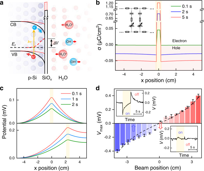
Fig. 2. Local charge accumulation induced by light illumination.
a Schematic of the surface band bending of p-type Si and ion redistribution in the water. VB, CB, Ef, and ΔV represent valence band, conduction band, fermi level and surface potential change, respectively. The red dashed lines highlight the change of energy band upon light illumination. b Time evolution of simulated charge-density distribution along the silicon strip while a light beam illuminates at the center of a silicon strip, as highlighted by the yellow shade. Negative value means the accumulation of holes (as shaded by red color) and positive represents the accumulation of electrons. The left-top inset represents corresponding circuit model (see details in Supplementary Fig. 9). c Time evolution of simulated potential distribution while the light beam illuminates at the center (top panel) and off the center (bottom panel), as highlighted by the yellow shades. d Dependence of pulsed-light-induced peak voltage on the illuminating position away from the strip center. The vertical error bars indicate standard deviation of the measured peak values. The black dashed line is from numerical simulation. Insets are typical voltage responses to light beam on/off at positions marked by the arrows. The beam-on period is marked by yellow shade and the beam width is 5 mm.

