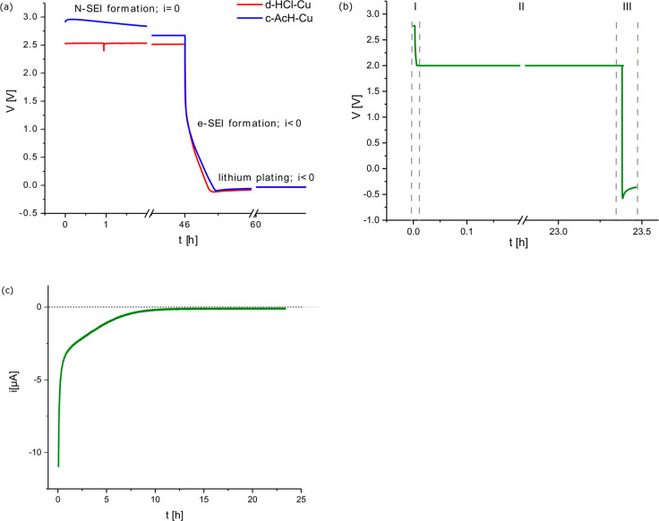
Figure 1.
(a) A typical voltage response, after cell assembly, for Cu-Li half cells made with the two Cu surface treatments, d- HCl and c-AcH. The rest period at OCV is followed by galvanostatic SEI formation and Li deposition on Cu using a 0.03 mA cm–2 current density (normalized to the Cu WE area). This procedure was used to prepare the samples for SEM and XPS. (b) A typical voltage response during SEI formation on Cu using 0.03 mA cm–2 current density, between OCV and 2 V (I), followed by eSEI2V formation during a voltage hold at 2 V (II) and galvanostatic Li deposition using 1.2 mA cm–2 current density (III). (c) A typical current response during the constant voltage hold at 2 V (denoted as stage II in (b)). The data presented in (b) and (c) are measured on c-AcH-Cu. The profile depicted in (b) was used to prepare the samples for ToF-SIMS.

