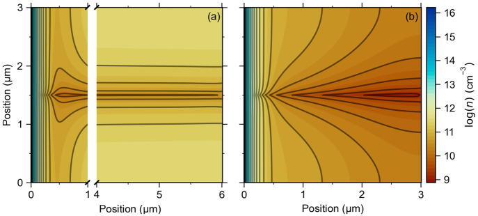
Figure 4.
Numerical calculations of the electron density contour maps at open-circuit voltage for (a) a 6 μm thick cell under uniform photogeneration (G = 6.3 × 1020 cm–3 s–1) and (b) a 3 μm thick cell under solar illumination containing a single grain boundary intersecting the n-type CdS layer (at the left edge) at its center. The solid (dark gray) lines are guides for the reader’s eye and illustrate the electron density contours. The grain boundary contains a single donor with a defect density Ngb = 1010 cm–2 and a recombination velocity S = 106 cm/s and is located at 0.85 eV (for uniform photogeneration) and at 0.75 eV (for solar illumination) below the conduction band edge, respectively. All calculations are done for μe = 100 cm2/(V s) and μh = 80 cm2/(V s); the simulation parameters are given in Table 1.

