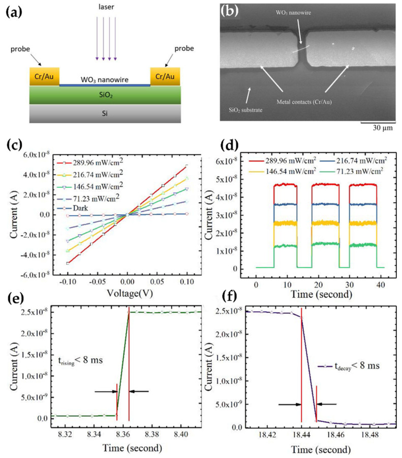
Figure 6.
(a) Sketch of the WO3 nanowire device structure; (b) SEM image of the WO3 nanowire device. (c) Current-voltage curves and (d) photo-switching behavior of the WO3 nanowires photodetector under the illumination of a 404 nm laser with different laser intensities. (e,f) are the rising time and decay time of the WO3 nanowire photodetector. Reproduced or adapted from [27].

