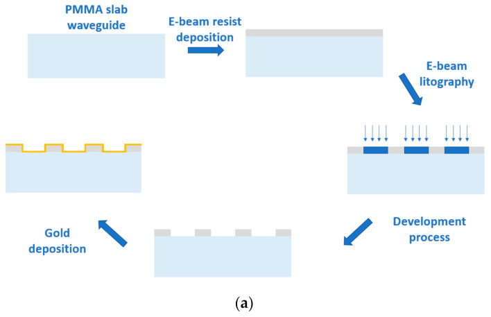
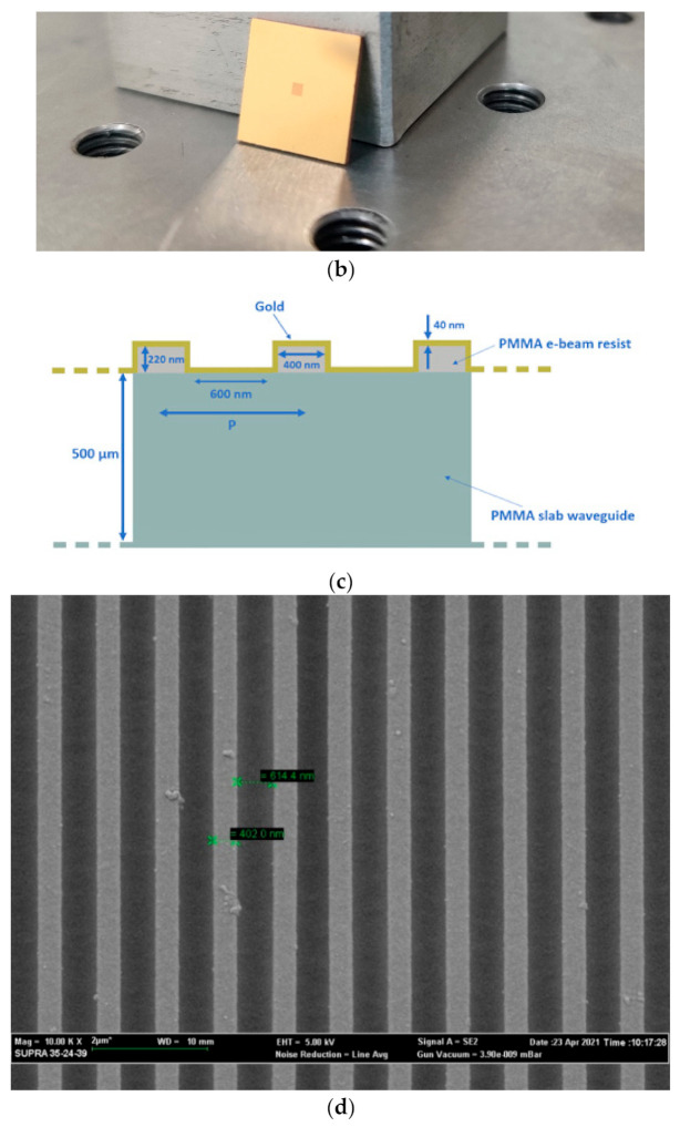
Figure 1.
(a) Outline of the fabrication process of the plasmonic sensor. (b) picture of the PMMA slab waveguide with gold nanograting pattern at the center. (c) Schematic cross section of the examined plasmonic GNG-based chip with the relative dimensions. (d) SEM image of the fabricated nanograting.


