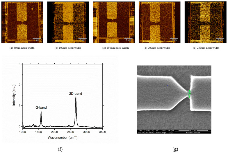
Figure 3.
AFM images of the graphene geometric diode (the black area is graphene) with different neck widths. (a) 50 nm neck width, (b) 100 nm neck width, (c) 150 nm neck width, (d) 200 nm neck width, (e) 250 nm neck width, (f) Raman spectrum of the graphene in the gap, (g) SEM image of the 50 nm neck width geometric diode.

