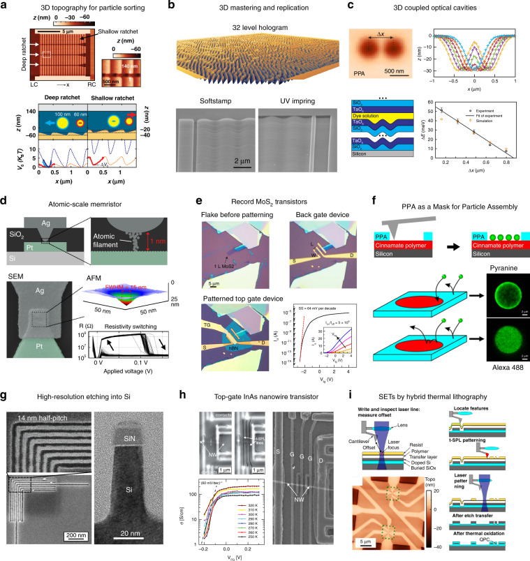
Fig. 4. Examples of applications achieved by material removal using t-SPL.
a 3D nanofluidic rocking Brownian motor sorting device for nanoparticles patterned into PPA resist. Reprinted with permission from ref. 56, AAAS. b Top: 32-level hologram in PPA, Bottom: a 300 nm deep sine wave used as master for UV nanoimprint. Reprinted with permission from ref. 31. c Gaussian-shaped optical microcavities patterned into PPA and etched into a Bragg mirror form photonic molecules. Adapted under CC BY 4.0 License from ref. 54, Copyright 2017 Springer Nature. d Atomic scale memristor devices fabricated by etching a cone-shaped t-SPL indent from PPA into SiO2. Adapted under CC BY 4.0 License from ref. 65, Copyright 2019 Springer Nature. e Single-layer MoS2 top gate transistor with record low contact resistance and on-off ratio. Reprinted with permission from ref. 68, Copyright 2019 Springer Nature. f Selective removal of PPA for accessing a functional material to study nanoparticle assembly processes. Reproduced with permission from ref. 72, Copyright 2018 ACS. g Left: 14 nm half-pitch pattern etched into Si. Reproduced with permission from ref. 29, Copyright 2017 ACS. Right: TEM image of a Si fin etched from patterned and Al2O3-infiltrated PPA resist. Adapted with permission from ref. 75, Copyright 2018 ACS. h InAs nanowire transistor overlaid with t-SPL-patterned metal top gate electrodes. Reprinted with permission from refs. 76,77, Copyright 2019 IEEE. i Integration of t-SPL with a laser writer for fabrication of Si-based room temperature single-electron transistors. Reproduced with permission from ref. 43, Copyright 2018 IOP Publishing

