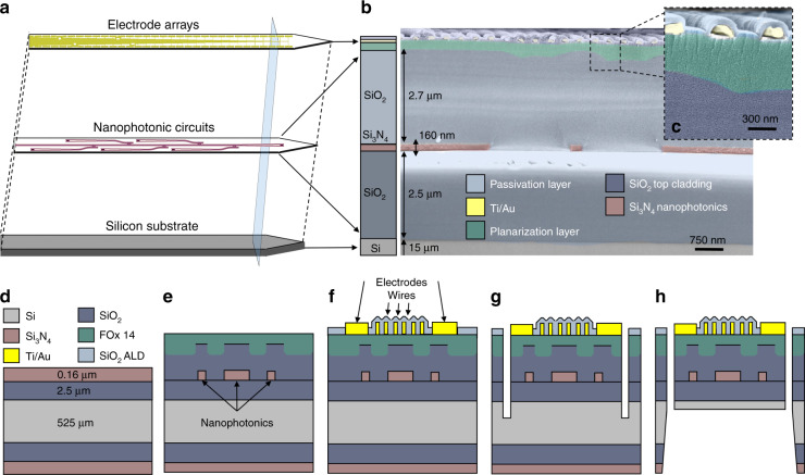
Fig. 3. Schematics of the integrated device and its fabrication process.
a Stacking of the nanophotonic circuits and electrode arrays. b False-color SEM cross-section, with the corresponding scheme on the left, highlighting the different layers. The scale bar is 750 nm. c High magnification of the top layers in (b), showing the planarization layer and wires. The scale bar is 300 nm. Fabrication steps: d Initial silicon wafer (525 µm), with 2.5 µm of LPCVD SiO2 and 160 nm optical grade Si3N4 layers. e Patterning of nanophotonic circuits, optical insulation, and planarization using a flowable oxide (FOx 14). f Integration of the arrays of electrodes and wires above the nanophotonic circuits, followed by passivation with 60 nm of ALD-grown SiO2. g Patterning of the device shape. h Release of the device by backside etching, which removes most of the underneath silicon and yields an overall probe thickness of 20 µm

