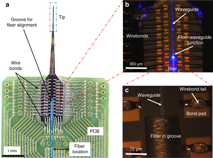
Fig. 4. Optical microscope images of the probe after connecting its nanophotonic circuits and arrays of sensors to external instrumentation.
a Device electrical connection. The whole device is shown, consisting of the tip and the interface area, which has bonding pads and an alignment groove for the optical fiber. The probe is glued onto a custom-made printed circuit board (PCB) and wire bonded. The scale bar is 1 mm. b Magnification of (a) showing the optical junction between the fiber and the waveguide, as well as the wire bonding and groove area. The laser is on, and the waveguide (in blue) is visible due to sidewall scattering. The scale bar is 350 µm. c Close-up image of the fiber-waveguide edge junction, highlighting details of the fiber, waveguide, and surrounding bonded pads. The scale bar is 75 µm

