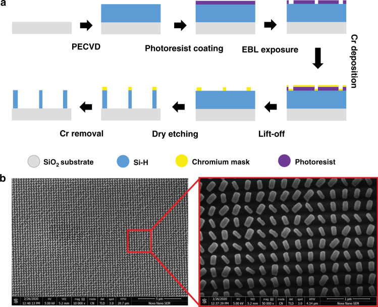
Fig. 5. Fabrication steps and SEM images of the metasurface.
a The metahologram was fabricated through the PECVD process. First, an a-Si:H layer was grown on top of a 500-μm thick SiO2 substrate. The deposition rate of a-Si:H was controlled by managing the flow rates of saline (SiH4) and hydrogen (H2) gases. The a-Si:H nanorods were defined by electron-beam lithography on a positive-type photoresist. A 30-nm thick chromium (Cr) layer was deposited followed by the lift-off process. The geometrical arrangement was transferred to a-Si:H using the Cr mask and dry etching. b SEM images of the designed asymmetric wavefront generation metasurface. The right image shows a magnified view of our fabricated hydrogenated noncrystalline silicon nanoresonators on top of a SiO2 substrate.

