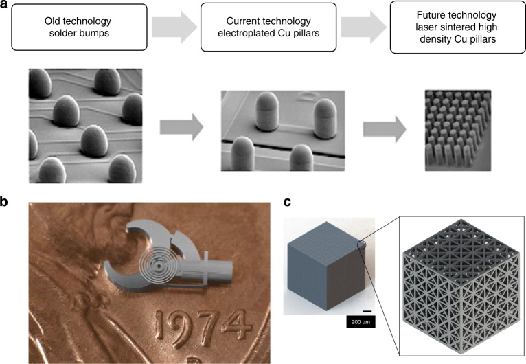
Fig. 1. Potential applications of the μ-SLS process.
a Evolution of C4 solder bumps(adapted from ref. 33)- The previous technology used ~1:1 aspect ratio SnAg bumps with >100 μm diameter features and >150 μm pitch. Current state-of-the-art technologies use sub-100 μm electroplated copper pillars to reduce the overall footprint of ICs. However, the process limitations of electroplating make it difficult to fabricate large-area, high aspect ratio sub-50 μm resolution structures. The μ-SLS process can enable the fabrication of the next generation of copper pillar-like structures with applications in flip-chip electronics industry. b Ni-Co compliant microforceps fabricated using a hybrid-AM technology useful in minimally invasive microsurgeries (adapted from ref. 34. Reproduced with permission from Emerald Publishing Limited). The high throughput capabilities of μ-SLS process can drive the production scale fabrication of essential microproducts like these. c A representation of large-area fabrication potential (1.2 × 1.2 × 1.2 mm3) of the μ-SLS process. Complex lattice-like microstructures (inset) have applications in developing extremely lightweight structural elements.

