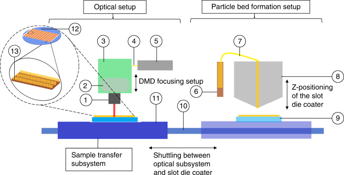
Fig. 2. A simplified schematic of the μ-SLS process showing the different subsystems involved in layer-by-layer fabrication of a true-3D structure. Optical Setup.
1 – Secondary focusing optics. 2 – Primary beam-shaping optics for the Digital Micromirror Device (DMD) array. 3 – DMD array housing and controller. 4 – Optical fiber coupling the laser driver output and DMD array. 5 – CW Laser driver; Particle bed formation setup. 6 – Syringe pump for nanoparticle ink transfer into the slot die coater. 7 – Slot die coater tubing for fluid intake, aspiration, and distribution. 8 – Die head coupled with a vertical positioner for adjusting the coating gap in between layers. 9 – Heated vacuum chuck with the substrate/wafer; Sample Transfer Subsystem. 10 – Direct drive linear motor for shuttling the wafer between optical setup and slot die coating setup. 11 – XY-Nanopositioner for wafer alignment and stepping during large-area fabrication. 12 – A representation of wafer scale fabrication of the 3D parts. 13 – Enlarged view of the individual patterns formed by the μ-SLS process.

